Non-volatile semiconductor storage device

a semiconductor storage device and non-volatile technology, applied in semiconductor devices, digital storage, instruments, etc., can solve the problems of physical improvement limit, such as the breakdown voltage between devices, and the cost of lithography process is ever increasing, and achieves the effect of increasing the breakdown voltag

Active Publication Date: 2011-08-30
KIOXIA CORP
View PDF11 Cites 269 Cited by
  • Summary
  • Abstract
  • Description
  • Claims
  • Application Information

AI Technical Summary

Problems solved by technology

Although it is common to reduce (refine) the dimension for each device for increased memory storage capacity, recent years are facing challenges in such refinement from the viewpoint of cost and technology.
However, the costs of lithography process are ever increasing.
In addition, if such refinement is accomplished, it is assumed that physical improvement limit, such as in breakdown voltage between devices, would be reached unless driving voltage can be scaled.
That is, it is likely that difficulties would be encountered in device operation itself.
However, Japanese Patent Laid-Open No. 2007-317874 requires word lines to be formed separately for each memory string, which poses a problem that the wiring resistance of the word lines cannot be reduced.

Method used


Image

  • Non-volatile semiconductor storage device
  • Non-volatile semiconductor storage device
  • Non-volatile semiconductor storage device

Examples


first embodiment

Configuration of Non-Volatile Semiconductor Storage Device 100 in First Embodiment

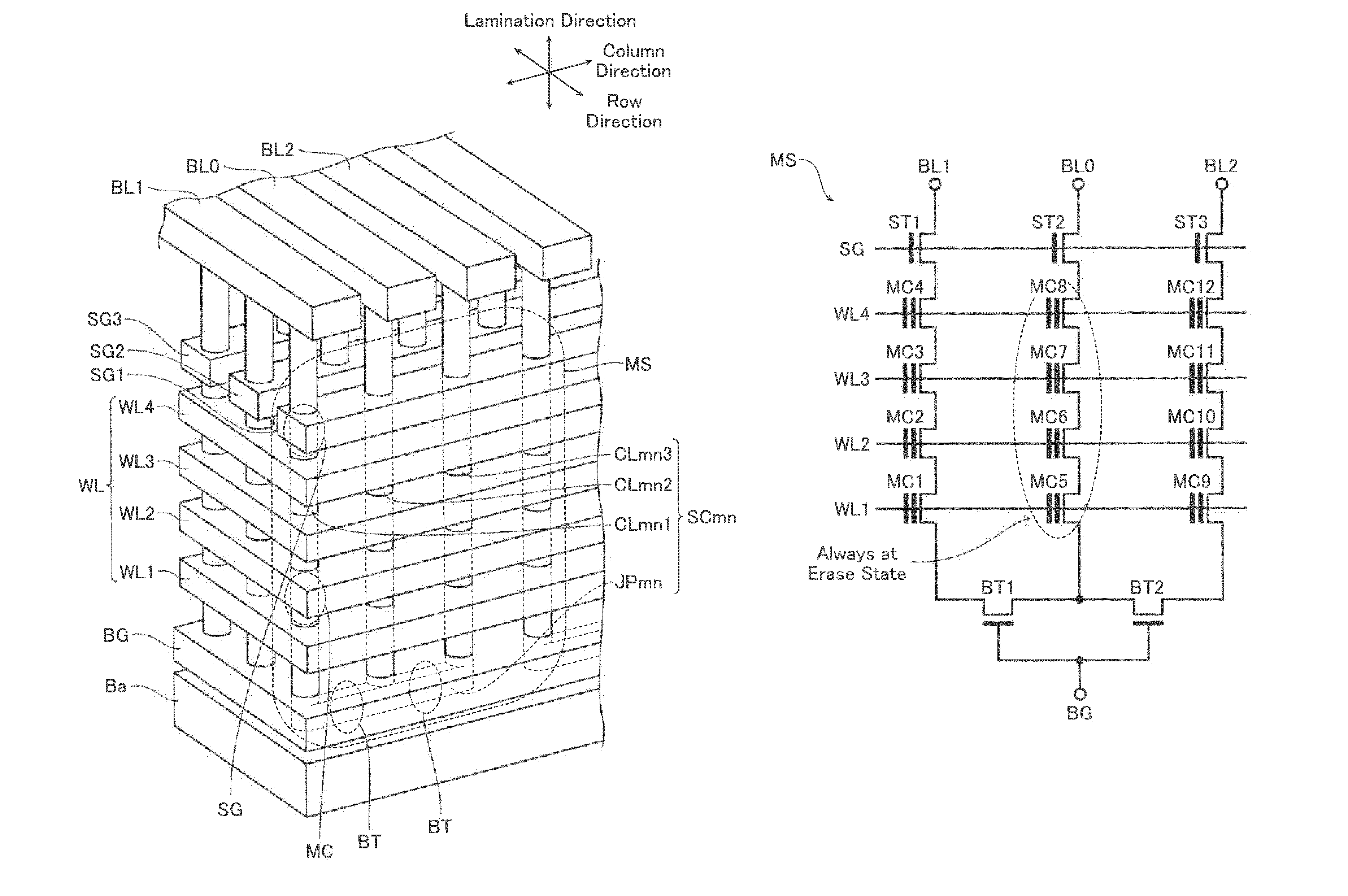
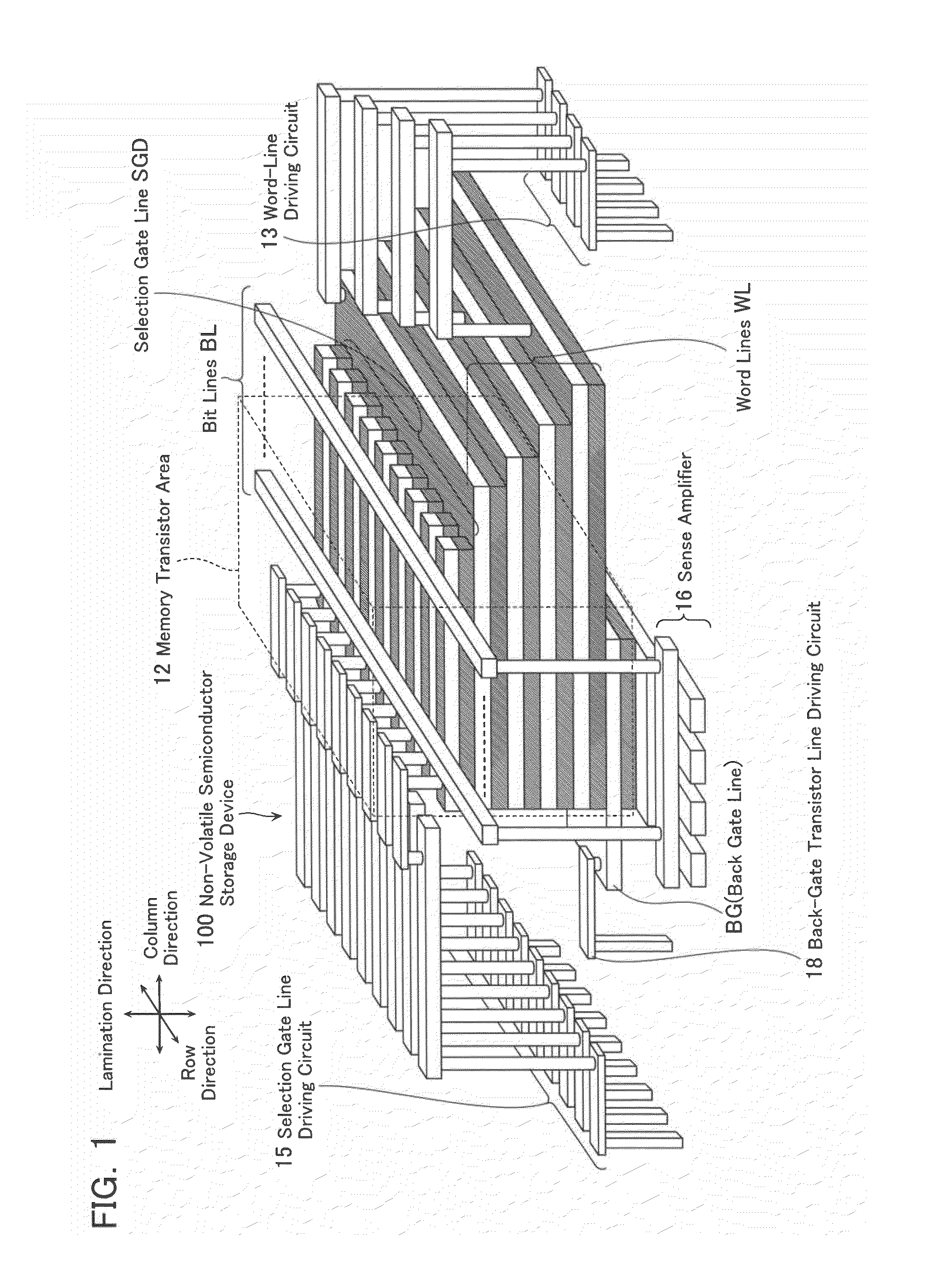
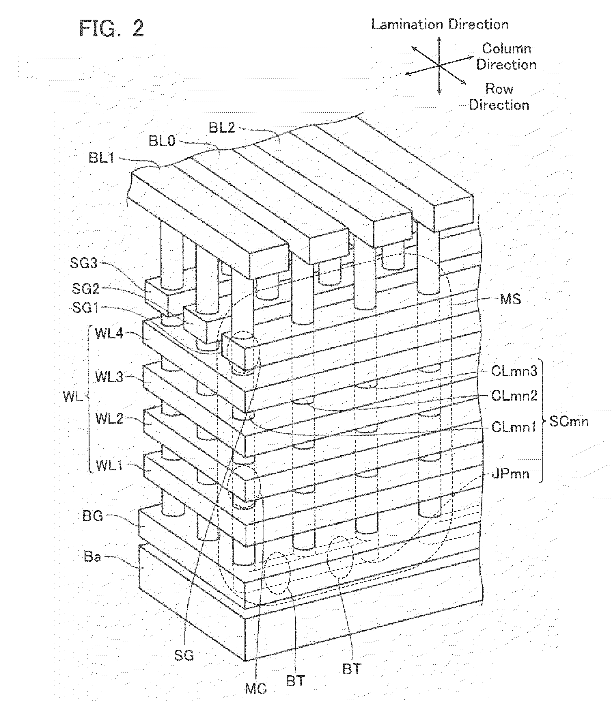
[0031]FIG. 1 schematically illustrates a non-volatile semiconductor storage device 100 according to a first embodiment of the present invention. As illustrated in FIG. 1, the non-volatile semiconductor storage device 100 according to the first embodiment mainly comprises: a memory transistor area 12; a word-line driving circuit 13; a selection gate line driving circuit 15; a sense amplifier 16; and a back-gate transistor driving circuit 18.

[0032]The memory transistor area 12 has memory transistors for storing data. The memory transistors are connected in series to provide memory strings, as discussed below. In addition, selection transistors are connected to the opposite ends of the memory strings. The word-line driving circuit 13 controls voltage applied to word lines WL. The selection gate line driving circuit 15 controls voltage applied to selection gate lines SG.

[0033]The sense amplifier 16 amplifi...

second embodiment

[0106]FIG. 17 schematically illustrates the memory transistor area 12 in the non-volatile semiconductor storage device 100 according to a second embodiment of the present invention. FIG. 18 is a plan view thereof. Note that the same reference numerals represent the same components as the first embodiment and description thereof will be omitted below.

[0107]While this embodiment involves the selection gate lines SG1 to SG8, among these, the odd-numbered selection gate lines SG1, SG3, SG5, and SG7 are formed in lower layers, and the even-numbered selection gate lines SG2, SG4, SG6, and SG8 are formed at positions in between, and above, the respective odd-numbered selection gate lines.

[0108]The two-layer alternating type selection gate line structure as mentioned above allows the area to be 4 F2 for each columnar portion CLmn.

[0109]Note that the number of columnar portions CLmn included in one memory string MS is not limited to three, but may be any number not less than two. Here, a rel...


PUM


Abstract

A memory string has a semiconductor layer with a joining portion that is formed to join a plurality of columnar portions extending in a vertical direction with respect to a substrate and lower ends of the plurality of columnar portions. First conductive layers are formed in a laminated fashion to surround side surfaces of the columnar portions and an electric charge storage layer, and function as control electrodes of memory cells. A second conductive layer is formed around the plurality of columnar portions via a gate insulation film, and functions as control electrodes of selection transistors. Bit lines are formed to be connected to the plurality of columnar portions, respectively, with a second direction orthogonal to a first direction taken as a longitudinal direction.

Description

CROSS REFERENCE TO RELATED APPLICATIONS[0001]This application is based on and claims the benefit of priority from prior Japanese Patent Application No. 2008-207655, filed on Aug. 12, 2008, the entire contents of which are incorporated herein by reference.BACKGROUND OF THE INVENTION[0002]1. Field of the Invention[0003]The present invention relates to an electrically rewritable non-volatile semiconductor storage device.[0004]2. Description of the Related Art[0005]Conventionally, LSIs are formed by integration of devices in a two-dimensional plane on the silicon substrate. Although it is common to reduce (refine) the dimension for each device for increased memory storage capacity, recent years are facing challenges in such refinement from the viewpoint of cost and technology. Such refinement requires further improvements in photolithography technology. However, the costs of lithography process are ever increasing. In addition, if such refinement is accomplished, it is assumed that phys...

Claims


Application Information

Patent Timeline
Patent Type & Authority Patents(United States)
IPC IPC(8): H01L29/792
CPCG11C5/02G11C5/025G11C5/063G11C8/14G11C16/0483H01L27/11565H01L27/11578H01L27/11582H01L29/42348H01L29/792H01L29/7926H10B43/10H10B43/20H10B43/27H01L29/0688
Inventor FUKUZUMI, YOSHIAKIKATSUMATA, RYOTAKITO, MASARUKIDOH, MASARUTANAKA, HIROYASUISHIDUKI, MEGUMIKOMORI, YOSUKEAOCHI, HIDEAKI
Owner KIOXIA CORP
Why Eureka
Try Eureka