Planar capacitor memory cell and its applications

a capacitor memory cell and capacitor technology, applied in the field of random access memory, can solve the problems of increasing die area, consuming more power of generators, and difficulty in obtaining necessary capacitance, and achieve the effects of less complicated fabrication, high current gain, and high performan

Inactive Publication Date: 2007-04-24
KIM JUHAN
View PDF13 Cites 270 Cited by
  • Summary
  • Abstract
  • Description
  • Claims
  • Application Information

AI Technical Summary

Benefits of technology

[0014]In the present invention, a planar capacitor memory cell and its applications are described. The memory cell includes a capacitor and a diode which are less complicated to fabricate, and does not need complex MOS access device. Capacitor includes silicon dioxide or high dielectric insulator, and plate of capacitor couples to storage node which has no coupling region to other nodes. In doing so, plate can swing ground to supply level to write data. Diode has four terminals where first terminal serves as word line, second terminal is storage node, third terminal is floating and fourth terminal serves as bit line. Diode need not be a high performance device nor have a high current gain. After storing data, diode is turned-off to cut off standby current. As a result, the present invention has many advantages as follows.
[0015]The memory does not use negative voltage for switching. Single or dual positive voltage can operate all the memory arrays. And memory cell does not need holding current to sustain data. In this manner, very low power consumption is realized.
[0016]The memory has long retention time. Low power consumption suppresses temperature, which can reduce junction leakage and capacitor oxide leakage. It is very helpful to store data for a long time in the storage node with low leakage, which can increase memory yield. And there is no need of big capacitor because the storage capacitor drives the base of bipolar transistor to read the stored data instead of heavily loaded bit line, while the diode drives heavily loaded bit line directly. Capacitor oxide leakage is minimized with low leakage material or thick oxide. One more leakage path is through third terminal, which forms a parasitic MOS transistor such that substrate serves as a gate, third terminal serves as a body, second terminal which is storage node serves as source or drain, and fourth terminal serves as drain or source. It is so-called back channel effect on SOI (Silicon-on Insulator) type planar device. This path can be carefully controlled by adding majority carrier into third terminal, or applying negative voltage to the substrate, where negative voltage generator has very low power consumption because it compensates insulator leakage, not switching current. And leakage of storage node through reverse bias can be reduced with low concentration doping to form diode while MOS transistor needs high doping drain and source. In this manner, all leakage paths can be reduced.
[0019]The memory operation is very fast and stable. Diode output can be transferred to latch device quickly, because diode current is generally much higher than that of MOS transistor. Furthermore, the diode also serves as a sense amplifier such that the diode generates binary value “on” or “off”, whether the storage node (the second terminal) is forward-bias or not, comparing to the voltage of the word line. Thus, diode can replace sense amplifier. And non destructive read is realized by sustaining the current path with NMOS pull-down, which need not restoring procedure and makes to reduce cycle time. However, in some applications, destructive read is still useful to make compatibility with conventional DRAM, which does not need to sustain the current path with NMOS pull-down when reading, but needs restoring procedure for each read. Write operation has a sequence to clear data, that is, to turn-on diode before writing, which makes storage node to have the same starting voltage when writing. Without this sequence, the stored level depends on the previous level which can be discharged after restored.

Problems solved by technology

In these days, DRAM has progressed its miniaturization and as a result there arises difficulties in obtaining necessary capacitance, in decreasing leakage current at turn-off of access transistor, and in holding data charge.
And those generators consume more power and increase die area.
Disadvantages are that the holding current is too high for all memory cells even though each memory cell has very little current, and relatively high voltage is required to make avalanche multiplication.
One of disadvantage is that the charge plate 435 should be negative bias voltage during standby.
Second word line 437 has very high switching current, which signal stays at negative level to store data during standby, then moves from negative to high level to write cells, and consequently consumes high power with internal negative voltage generator.
Moreover, this prior part of memory cell in FIG. 4 has one more disadvantage to sustain latched-up data by subthreshold current, if holding current is higher than subthreshold current, memory cell loses data.
However, this prior art of cell needs complexity of operation using negative voltage, and needs MOS device to read which is more complicated to shrink.
However, these cells need negative voltage for read and write operations, and write time is relatively slow to generate ions by impact ionization, which takes 5 ns to 10 ns, as published.

Method used


Image

  • Planar capacitor memory cell and its applications
  • Planar capacitor memory cell and its applications
  • Planar capacitor memory cell and its applications

Examples


Embodiment Construction

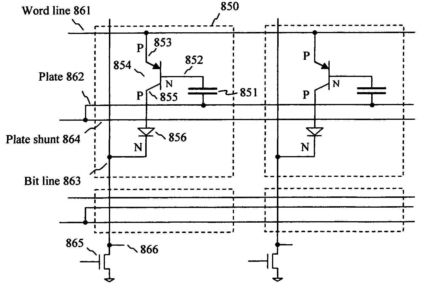
[0037]The present invention is directed to random access memory, which stores data in a storage capacitor. In FIG. 7, the present invention of memory cell 700 is shown. The plate 762 only couples to base 752 which forms a storage capacitor 751, wherein the plate shunt 764 is added to reduce resistance of the plate 762. Generally, four-terminal diode (p-n-p-n diode, known as Shockley diode) is described as a p-n-p transistor and an n-p-n transistor which form a feedback loop. Once turned on, p-n-p-n diode will remain on conducting state with the feedback loop, as long as there is a significant current flowing through it. However, in the capacitor memory applications, one of two transistors is simplified as a p-n diode to remove feedback loop because the storage capacitor effectively controls the base of p-n-p transistor with the stored charge, while there is no storage capacitor in the base of n-p-n transistor. Hence, n-p-n transistor is replaced with a p-n junction. If storage node ...


PUM


Abstract

A capacitor memory is realized, wherein a capacitor stores data and a diode controls to store data “1” or “0”. Diode has four terminals wherein first terminal serves as word line, second terminal serves as storage node, third terminal is floating, and fourth terminal serves as bit line, wherein back channel effect is suppressed adding additional ions in the bottom side of third terminal or applying negative voltage in the well or substrate. A capacitor plate couples to second terminal, which plate has no coupling region to first, third and fourth terminal. With no coupling, the inversion layer of plate in the storage node is isolated from the adjacent nodes. In doing so, the plate can swing ground level to positive supply level to write. As a result, no negative generator is required for controlling plate. Word line and bit line keep ground level during standby, and rise to supply level for read or write operation. In this manner, no holding current is required during standby, and operating current is dramatically reduced with no negative generator. Write has a sequence to clear the state of cell before writing to store data regardless of previous state. Refresh cycle is periodically asserted to sustain data. The present invention can be applied for destructive read, or for nondestructive read adding pull-down device to bit line. The height of cell is almost same as control circuit on the bulk or SOI wafer.

Description

FIELD OF THE INVENTION[0001]The present invention relates generally to integrated circuits and in particular to a random access memory.BACKGROUND OF THE INVENTION[0002]An essential semiconductor device is semiconductor memory, such as a random access memory (RAM) device. A random access memory device allows the user to execute both read and write operations on its memory cells. Typical examples of RAM devices include dynamic random access memory (DRAM), static random access memory (SRAM), and cache memory.[0003]DRAM is a specific category of RAM containing an array of individual memory cells, where each cell includes a capacitor for holding a charge and a transistor for accessing the charge held in the capacitor. The transistor is often referred to as the access transistor or the transfer device of the DRAM cell.[0004]FIG. 1 illustrates a portion of a DRAM memory circuit containing a DRAM cell as a prior art. DRAM cell contains a storage capacitor 114 and an access field effect tran...

Claims


Application Information

Patent Timeline
Patent Type & Authority Patents(United States)
IPC IPC(8): G11C11/36
CPCH01L21/8221H01L21/84H01L27/0688H01L27/1023H01L27/105H01L27/108H01L27/1203G11C7/1051G11C7/106G11C7/12G11C11/22G11C11/24G11C11/404G11C11/405G11C11/4067G11C11/4085G11C11/4093G11C11/4094G11C13/0004G11C13/004G11C13/0069G11C15/043H01L27/1052G11C2013/0078G11C2211/4016G11C2213/72H01L27/101H01L27/1214H10B12/10H10B99/00H10B12/00
Inventor KIM, JUHAN
Owner KIM JUHAN
Why Eureka
Try Eureka