Heterojunction bipolar transistor with dielectric assisted planarized contacts and method for fabricating

a bipolar transistor and dielectric assisted technology, applied in the field of semiconductor devices, can solve the problems of increased interconnection complexity, inability to reliably contact high-speed hbts, increased interconnection complexity, etc., and achieve the effect of reliable semiconductor and readily reproducibl

Inactive Publication Date: 2005-09-27
TELEDYNE SCI & IMAGING
View PDF7 Cites 13 Cited by
  • Summary
  • Abstract
  • Description
  • Claims
  • Application Information

AI Technical Summary

Benefits of technology

[0016]The new device and method allows for fabricating devices without relying on etching conductive vias for contacting the contact metals. The new method results in devices that are more reproducible and reliable and less complicated to fabricate. Also, the size of the device is not limited by the resolution of the via etching. Smaller devices can be fabricated, which can result in faster devices that consumes less power.

Problems solved by technology

This design goal places a greater emphasis on increased component integration and packing density, which results in decreased feature sizes, increased interconnection complexity and use of new or specialized materials.
One disadvantage of this technique is that it cannot be used to reliably contact high speed HBTs.
The resolution and alignment limits of lithography and etch systems limit how small the device features can be for HBTs.
This naturally results in a greater number of fabrication errors, making the HBTs less reproducible.
Variations in feature height, topography or morphology can lead to stress in subsequently deposited layers or materials and height variations in one layer can make precise control of the dimensions of subsequent layers difficult.

Method used


Image

  • Heterojunction bipolar transistor with dielectric assisted planarized contacts and method for fabricating
  • Heterojunction bipolar transistor with dielectric assisted planarized contacts and method for fabricating
  • Heterojunction bipolar transistor with dielectric assisted planarized contacts and method for fabricating

Examples


Embodiment Construction

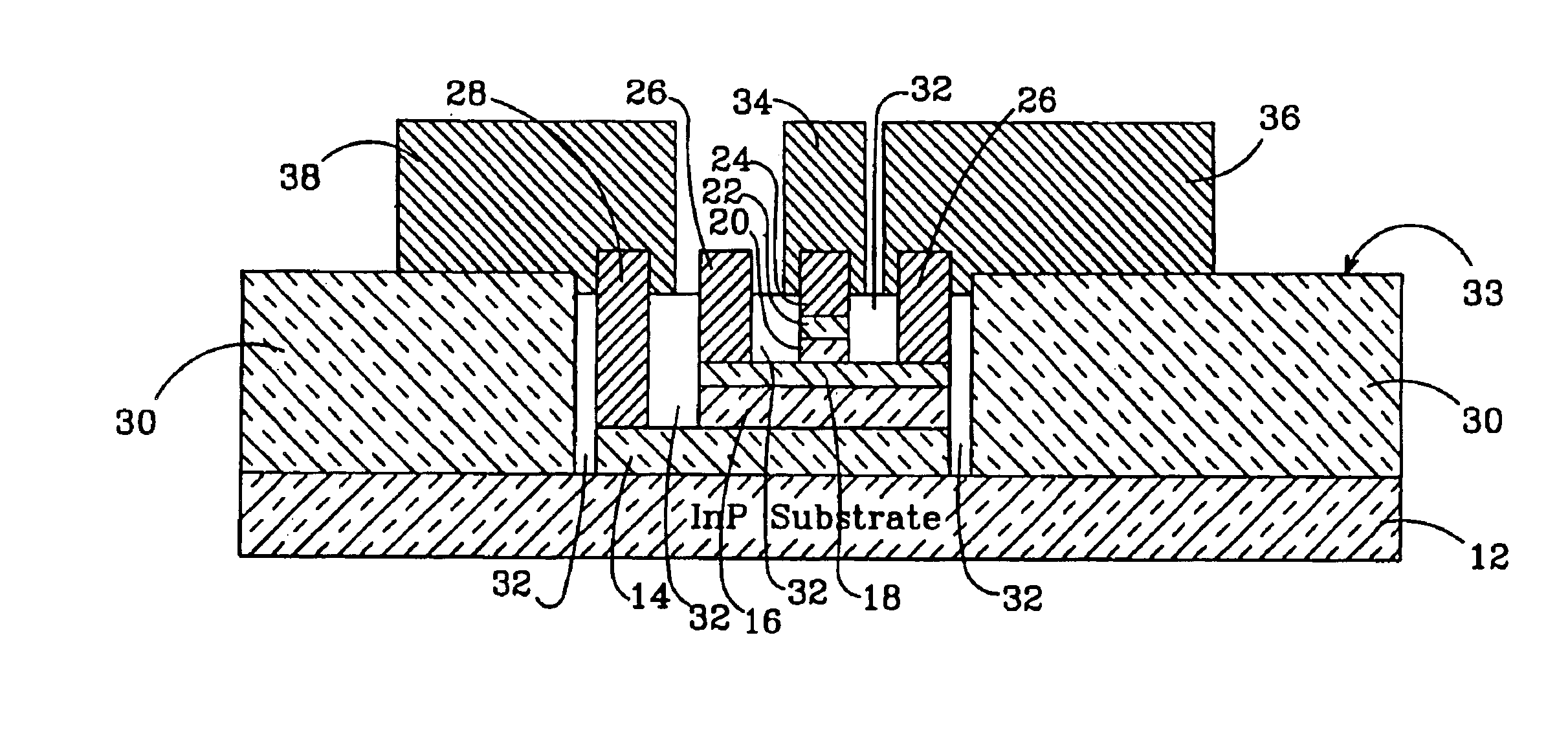
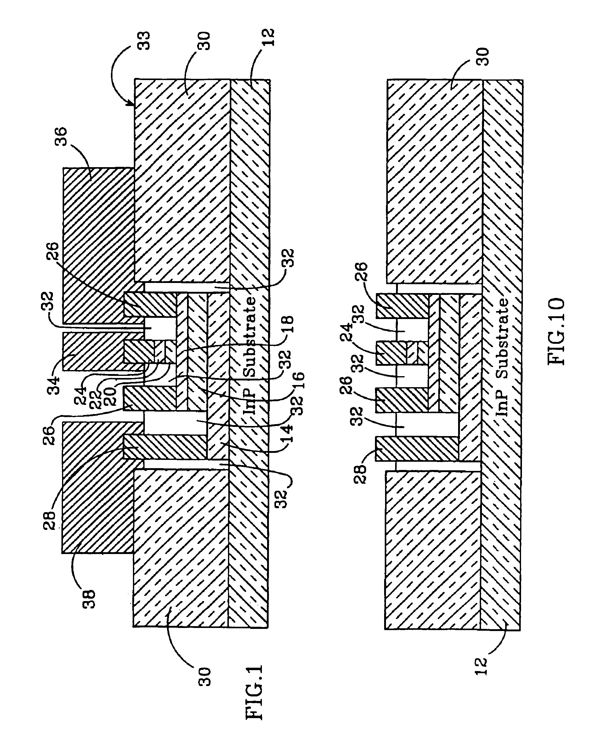
[0028]FIG. 1 shows one embodiment of an HBT 10 according to the present invention. It is formed on an electrically semi-insulating InP substrate 12, which supports an InP sub-collector 14, with the substrate extending laterally beyond the sub-collector layer 14. The sub-collector 14 is heavily doped n+ so that it is substantially conductive. The sub-collector 14 is typically about 0.5-1 micron thick, with a dopant concentration of greater than 1×10¹⁹ / cm3. The purpose of the sub-collector 14 is to establish an electrical contact with the collector layer 16, which normally directly contacts the upper surface of the sub-collector 14. The collector 16 is typically about 0.2-1.0 microns thick, with a dopant concentration of about 1×10¹⁶ to 1×10¹⁷ / cm3. The collector layer is typically doped with silicon (Si) during the epitaxial growth.

[0029]A heavily doped InGaAs base layer 18 is included on the collector layer 16 opposite the sub-collector layer 12, with the base layer 18 covering most ...


PUM

PropertyMeasurementUnit
widthaaaaaaaaaa
thickaaaaaaaaaa
thickaaaaaaaaaa

Abstract

A heterojunction bipolar transistor (HBT) is disclosed that includes successive emitter, base and collector and sub-collector epitaxial layers and emitter, base and collector contact metals contacting the emitter, base and sub-collector layers respectively. A passivation material is included that covers the uncovered portions of the layers and covers substantially all of the contact metals. The passivation material has a planar surface and a portion of each of the contact metals protrudes from the surface. Planar metals are included on the planar surface, each being isolated from the others and in electrical contact with a respective contact metal. A method for fabricating an HBT is also disclosed, wherein successive emitter, base, collector and sub-collector epitaxial layers are deposited on a substrate, with the substrate being adjacent to the sub-collector layer. The epitaxial layers are etched to provide locations for contact metals and emitter, base and contact metals are deposited on the emitter, base and sub-collector epitaxial layers, respectively. A self-alignment material is deposited on the surface of the substrate around the epitaxial layers and a planarization material is deposited on and covers the top surface of the HBT. The planarization material is then etched so it has a planar surface about the same level as the surface of the self-alignment material and the contact metals protrude from the planar surface. The planar metals are then deposited over the protruding portions of the contact metals.

Description

BACKGROUND OF THE INVENTION[0001]1. Field of the Invention[0002]This invention relates to semiconductor devices, and more particularly to planarized contacting of semiconductor devices such as high power heterojunction bipolar transistors (HBTs).[0003]2. Description of the Related Art[0004]HBTs are described in general in Wang, Introduction to Semiconductor Technology: GaAs and Related Compounds John Wiley & Sons, 1990, pp. 170-230. Some of the advantages of HBTs over other transistors such as FETs include; short transition times because of their vertical structure, higher current handling capability per unit chip area, which contributes to higher output drive capabilities, and increased transconductance.[0005]There is a continuing need to develop integrated circuits and components, including HBTs, which operate at higher frequency or speeds, with reduced power. This design goal places a greater emphasis on increased component integration and packing density, which results in decrea...

Claims


Application Information

Patent Timeline
Patent Type & Authority Patents(United States)
IPC IPC(8): H01L31/102H01L31/06H01L31/072H01L31/0264H01L31/0328H01L31/0336H01L31/109H01L21/331H01L29/737
CPCH01L29/66318H01L29/7371Y10S438/978
Inventor PIERSON, JR., RICHARD L.LI, JAMES CHINGWEIBRAR, BERINDER P. S.HIGGINS, JOHN A.
Owner TELEDYNE SCI & IMAGING
Why Eureka
Try Eureka