Silicon-on-insulator vertical array device trench capacitor DRAM

a vertical array device and trench capacitor technology, applied in the field of trench capacitor dynamic random access memory cells, can solve the problems soft errors, leakage, etc., and achieve the effect of reducing stored charge, reducing the risk of noise, and reducing the charge stored in the dram

Inactive Publication Date: 2003-05-20
GOOGLE LLC
View PDF28 Cites 290 Cited by
  • Summary
  • Abstract
  • Description
  • Claims
  • Application Information

AI Technical Summary

Problems solved by technology

Unfortunately, shrinking the capacitor plate area reduces capacitance and, consequently, reduces stored charge.
Reduced charge means that what charge is stored in the DRAM is more sus

Method used


Image

  • Silicon-on-insulator vertical array device trench capacitor DRAM
  • Silicon-on-insulator vertical array device trench capacitor DRAM
  • Silicon-on-insulator vertical array device trench capacitor DRAM

Examples


Embodiment Construction

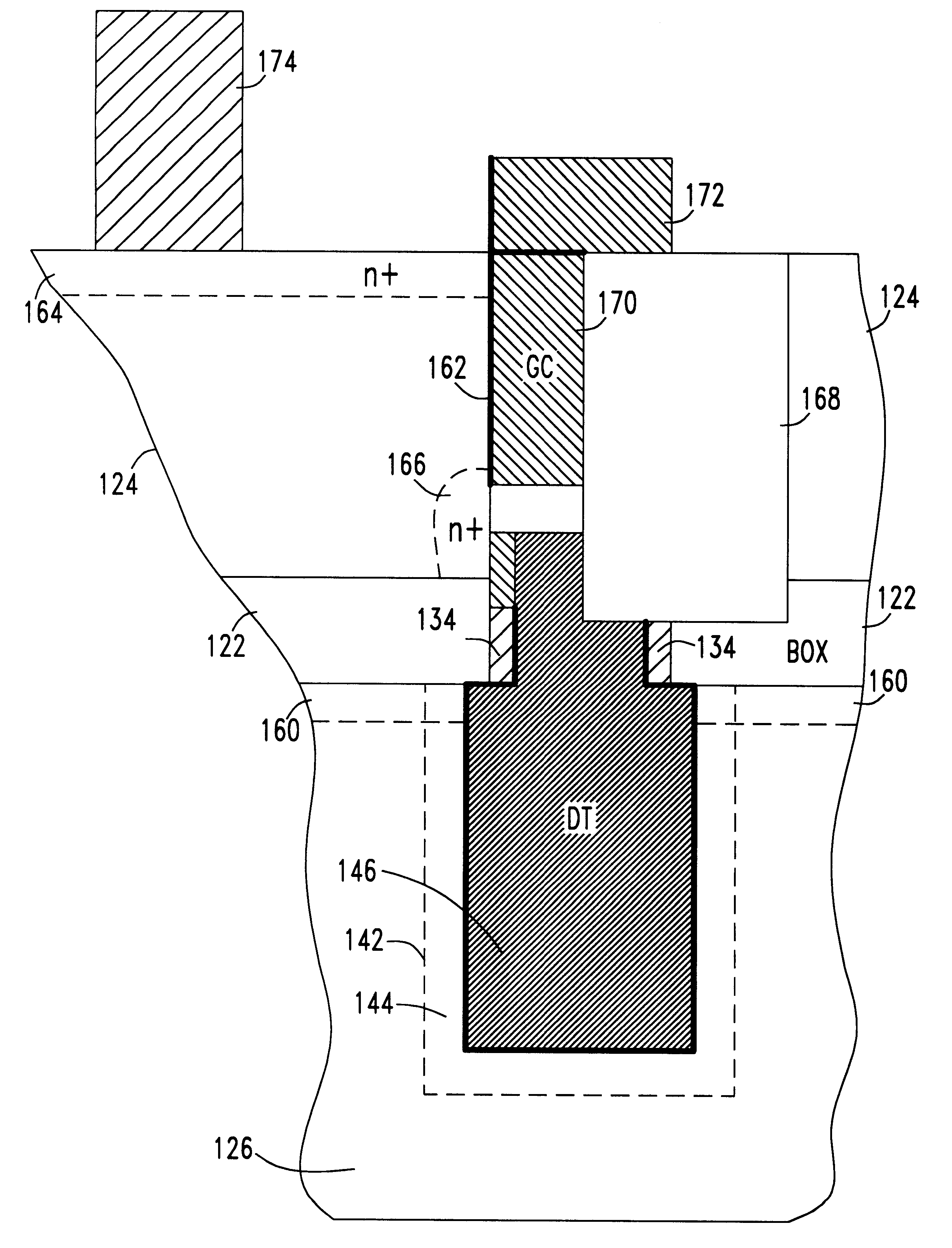
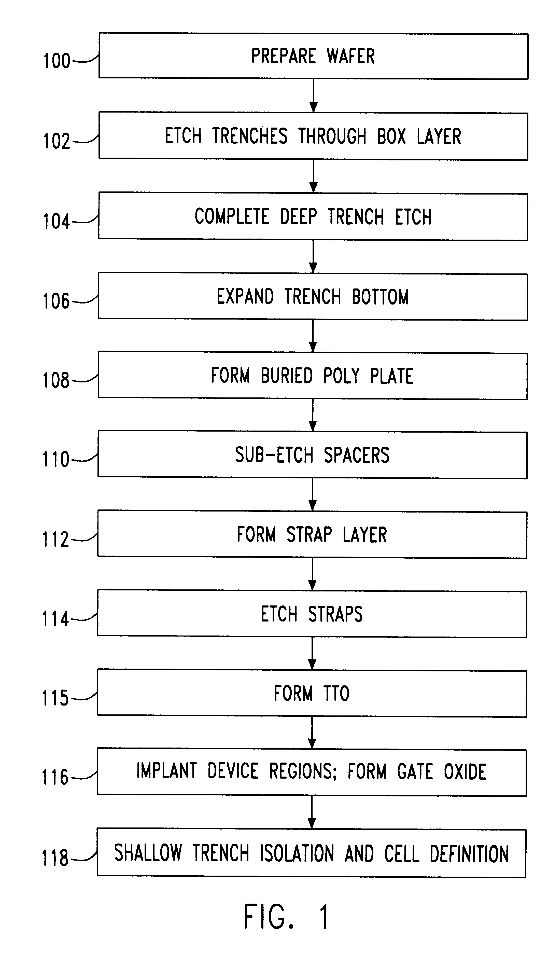
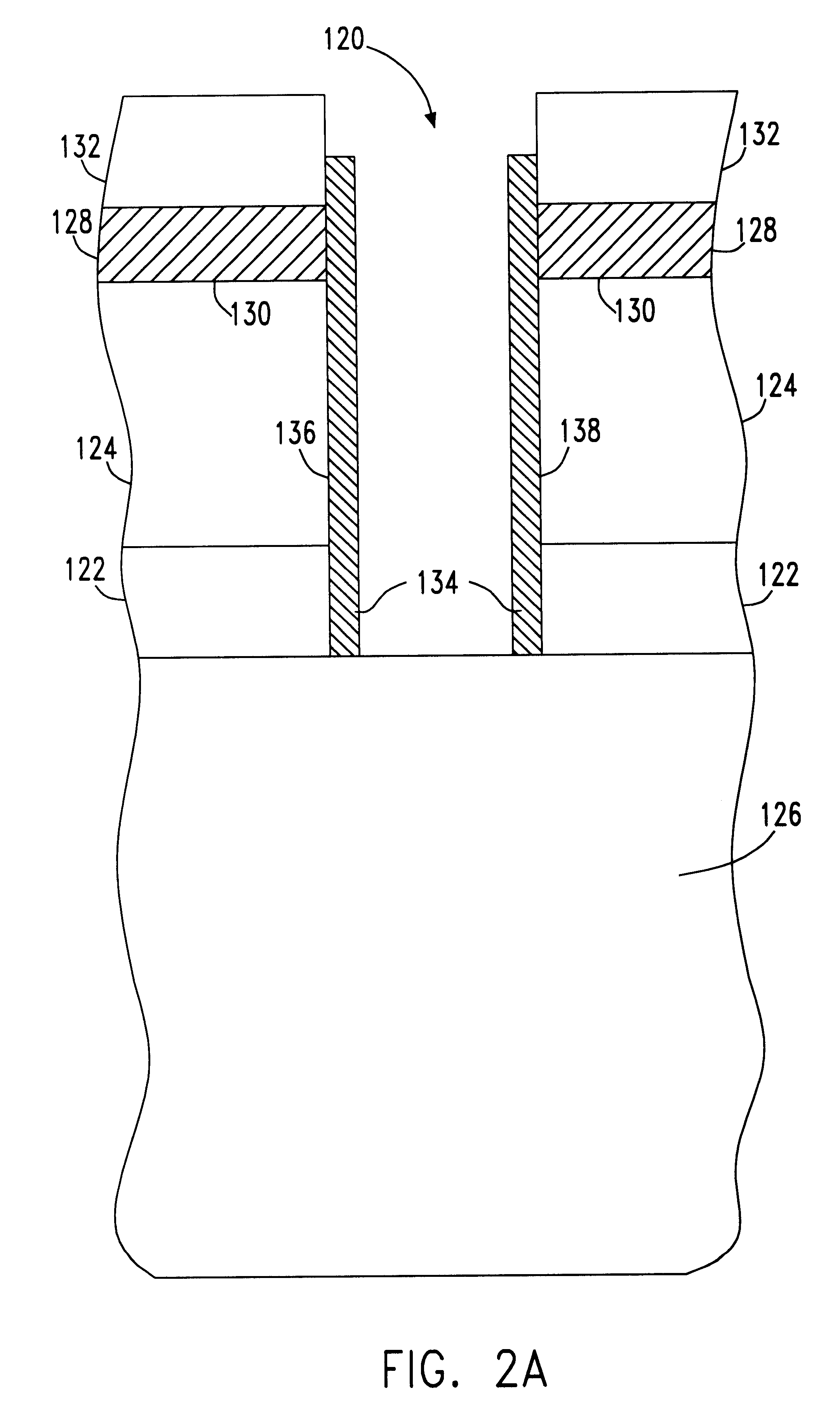
Referring now to the drawings, and more particularly, FIG. 1 shows a flow diagram of the preferred embodiment silicon-on-insulator (SOI) process for forming vertical DRAM cells. First, if a SOI wafer has not been previously prepared, then, in step 100, the SOI wafer is prepared from a semiconductor wafer. Preferably, the initial wafer is a single crystal silicon wafer. A buried oxide (BOX) layer is formed in the silicon wafer. The BOX layer isolates a silicon layer (SOI layer) above the BOX layer from a thick substrate below the BOX layer, which is much thicker than the silicon layer. Then, in step 102 a deep trench location pattern is formed, preferably, using a typical photolithographic process. Deep trenches are partially etched into the wafer, etching through the silicon layer and the BOX layer down to the thicker substrate. A protective spacer is formed along the sidewalls of the partially etched trenches to protect the SOI layer sidewalls. In step 104 the deep trenches are com...


PUM


Abstract

A silicon on insulator (SOI) dynamic random access memory (DRAM) cell and array and method of manufacture. The memory cell includes a trench storage capacitor connected by a self aligned buried strap to a vertical access transistor. A buried oxide layer isolates an SOI layer from a silicon substrate. The trench capacitor is formed in the substrate and the access transistor is formed on a sidewall of the SOI layer. A polysilicon strap connected to the polysilicon plate of the storage capacitor provides a self-aligned contact to the source of the access transistor. Initially, the buried oxide layer is formed in the wafer. Deep trenches are etched, initially just through the SOI layer and the BOX layer. Protective sidewalls are formed in the trenches. Then, the deep trenches are etched into the substrate. The volume in the substrate is expanded to form a bottle shaped trench. A polysilicon capacitor plate is formed in the deep trenches and conductive polysilicon straps are formed in the trenches between the capacitor plates and the SOI sidewalls. Device regions are defined in the wafer and a sidewall gate is formed in the deep trenches. Shallow trenches isolation (STI) is used to isolate and define cells. Bitlines and wordlines are formed on the wafer.

Description

1. Field of the InventionThe present invention generally relates to semiconductor memories and, more particularly, to a trench capacitor dynamic random access memory cell with a vertical silicon on insulator access transistor for semiconductor memories.2. Background DescriptionDynamic Random Access Memory (DRAM) cells are well known. A DRAM cell is essentially a capacitor for storing charge and a pass transistor (also called a pass gate or access transistor) for transferring charge to and from the capacitor. Data (1 bit) stored in the cell is determined by the absence or presence of charge on the storage capacitor. Because cell size determines chip density, size and cost, reducing cell area is one of the DRAM designer's primary goals. Reducing cell area is done, normally, by reducing feature size to shrink the cell.Besides shrinking the cell features, the most effective way to reduce cell area is to reduce the largest feature in the cell, typically, the area of the storage capacitor...

Claims


Application Information

Patent Timeline
IPC IPC(8): H01L21/70H01L21/8242
CPCH01L27/10864H01L27/1087H10B12/0383H10B12/0387
Inventor RADENS, CARL J.BRONNER, GARY B.CHEN, TZE-CHIANGDAVARI, BIJANMANDELMAN, JACK A.MOY, DANSADANA, DEVENDRA K.SHAHIDI, GHAVAM GHAVAMISTIFFLER, SCOTT R.
Owner GOOGLE LLC
Why Eureka
Try Eureka