Linearized conductive surface

a conductive surface, linear technology, applied in mechanical pattern conversion, instruments, computing, etc., can solve the problems of increasing the number of rows, increasing the touch panel border, and the inability of the electrode pattern to linearize the field

Inactive Publication Date: 2008-02-05
3M INNOVATIVE PROPERTIES CO
View PDF11 Cites 91 Cited by
  • Summary
  • Abstract
  • Description
  • Claims
  • Application Information

AI Technical Summary

Benefits of technology

[0015]In another aspect of the invention an article includes a plurality of conductive segments that are in contact with a conductive surface. The conductive segments are located along the edges of two or more concentric parallel polygo...

Problems solved by technology

Some electrode patterns may be incapable of linearizing the field to a level required in a given application.
Increasing the number of rows, however, tends to increase the touch panel border.
Therefore, improving field linearity may adversely affect the border size of a touch panel.
Such variations are typically unavoidable during manufacturing.
If small variations in the electrode pattern result in unacceptable nonl...

Method used


Image

  • Linearized conductive surface
  • Linearized conductive surface
  • Linearized conductive surface

Examples


example

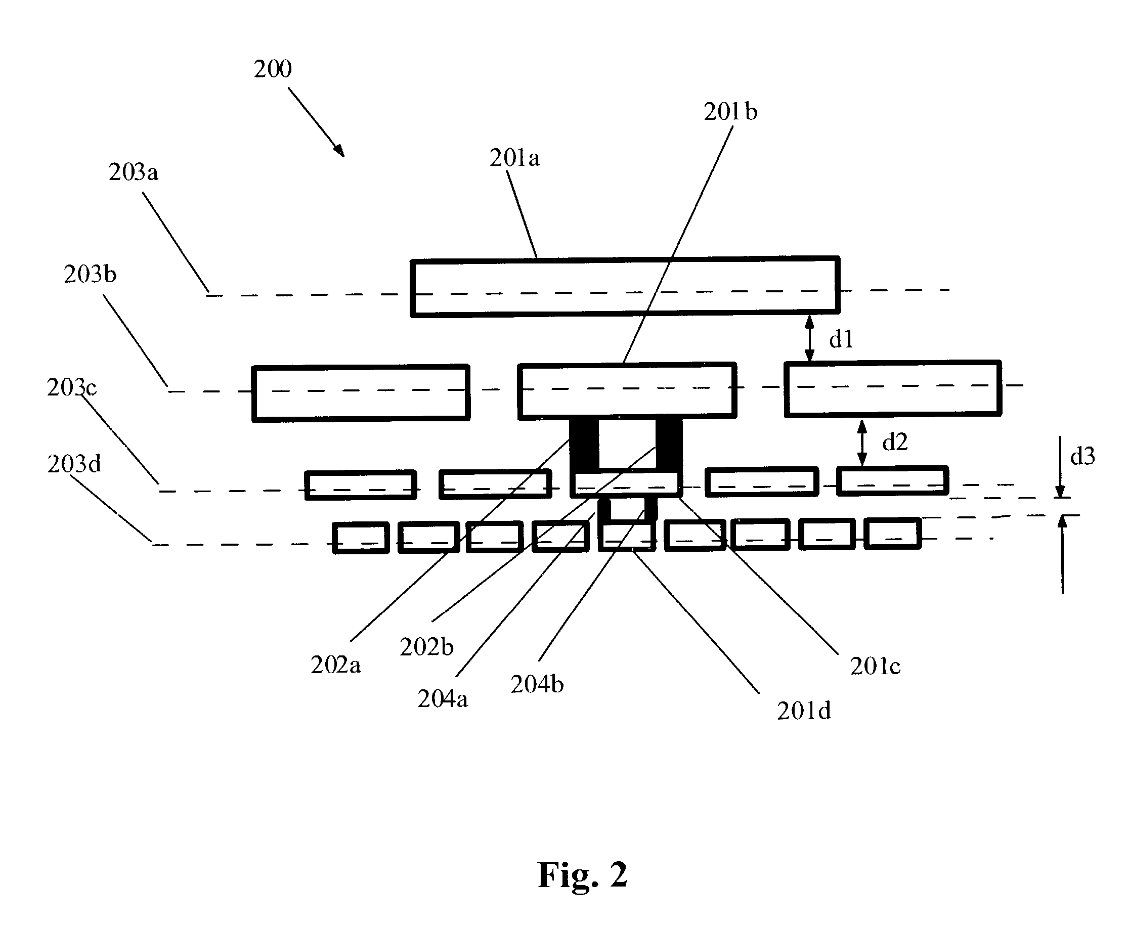
[0077]The electrode pattern 1000 shown in FIG. 10 was numerically modeled using a finite element analysis. The electrode pattern was incorporated in a capacitive touch sensor. The transparent conductor had a perimeter of 27.94 cm (long edge) by 21.59 ch (short edge), and had a sheet resistance of 2500 ohms per square. The sheet resistance of all conductive segments, connecting bars, and contact pads was 0.01 ohms per square. In addition, The following numerical values were used in modeling electrode pattern 1000 of FIG. 10:

[0078]separation between perimeter 1200 and row 1610 was 0.076 cm;

[0079]width of conductive segments in row 1610 was 0.063 cm;

[0080]separation between rows 1610 and 1620 was 0.038 cm;

[0081]width of conductive segments in row 1620 was 0.051 cm;

[0082]separation between rows 1620 and 1630 was 0.038 cm;

[0083]width of conductive segments in row 1630 was 0.038 cm;

[0084]separation between rows 1630 and 1640 was 0.038 cm;

[0085]width of conductive segments in row 1640 was ...


PUM


Abstract

Electrode pattern disposed on a conductive surface is disclosed. The electrode pattern includes a plurality of conductive segments. The conductive segments are located along the edges of two or more concentric parallel polygons. Each edge of each polygon has one or more middle segments disposed between two end segments. For each edge of each polygon the middle segments are equal in length, and the segments are equally spaced. A touch sensor is disclosed that includes such an electrode pattern.

Description

FIELD OF THE INVENTION[0001]This invention generally relates to forming a conductive electrode pattern on a transparent conductive surface. The invention is particularly applicable to linearizing an electric field on a conductive surface in a touch panel by forming an electrode pattern on and along the perimeter of the surface.BACKGROUND[0002]Touch screens allow a user to conveniently interface with an electronic display system. For example, a user can carry out a complicated sequence of instructions by simply touching the screen at a location identified by a pre-programmed icon. The on-screen menu may be changed by re-programming the supporting software according to the application.[0003]Resistive and capacitive are two common touch sensing employed to detect the location of a touch input. Resistive technology typically incorporates two transparent conductive films as part of an electronic circuit that detects the location of a touch. Capacitive technology, on the other hand, typic...

Claims


Application Information

Patent Timeline
IPC IPC(8): G06F3/041G06F3/045G06F3/044
CPCG06F3/045G06F2203/04113
Inventor KEEFER, KENNETH J.BULAT, BULENTGEAGHAN, BERNARD O.
Owner 3M INNOVATIVE PROPERTIES CO
Why Eureka
Try Eureka