Method of manufacturing a phase change RAM device utilizing reduced phase change current

a ram device and phase change technology, applied in the direction of semiconductor devices, electrical devices, nanotechnology, etc., can solve the problems requiring a high charge storage capability, and unable to achieve the high integration design of flash memories, so as to achieve the effect of reducing the current required

Active Publication Date: 2008-02-19
SK HYNIX INC
View PDF10 Cites 166 Cited by
  • Summary
  • Abstract
  • Description
  • Claims
  • Application Information

AI Technical Summary

Benefits of technology

[0020]Accordingly, the present invention has been made to solve the above-mentioned problems occurring in the prior art, and an object of the present invention is to provide a method of manufacturing a phase change RAM device capable of effectively lowering the current required for changing a phase of a phase change layer.

Problems solved by technology

However, although DRAM devices are generally known in the art to be superior memory devices, they require a high charge storage capability.
For this reason, the DRAM devices must increase the surface area of an electrode, and this requirement does not help high integration design of the DRAM devices.
This also does not help to achieve the high integration design of flash memories.
However, because the E-beam process is unstable, the bottom electrode 11 fabricated through the E-beam process cannot be uniformly formed throughout the predetermined area of the semiconductor substrate.
Thus, there are limitations in the conventional phase change RAM devices to reducing the contact area between the phase change layer and the bottom electrode, making these conventional devices difficult to lower the current required for changing the phase of the phase change layer.

Method used


Image

  • Method of manufacturing a phase change RAM device utilizing reduced phase change current
  • Method of manufacturing a phase change RAM device utilizing reduced phase change current
  • Method of manufacturing a phase change RAM device utilizing reduced phase change current

Examples


Embodiment Construction

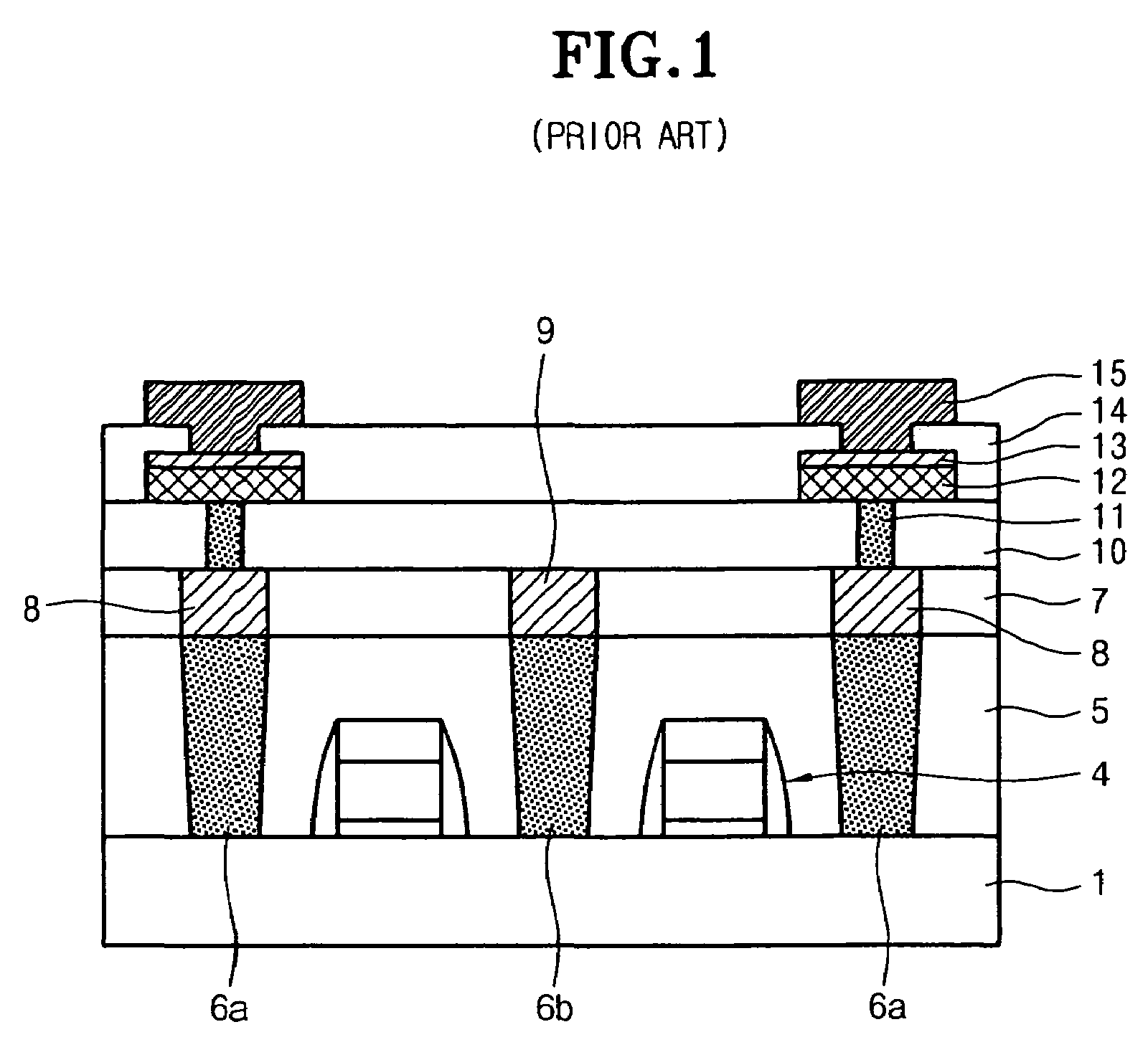
[0033]Hereinafter, the present invention will be described with reference to accompanying drawings.

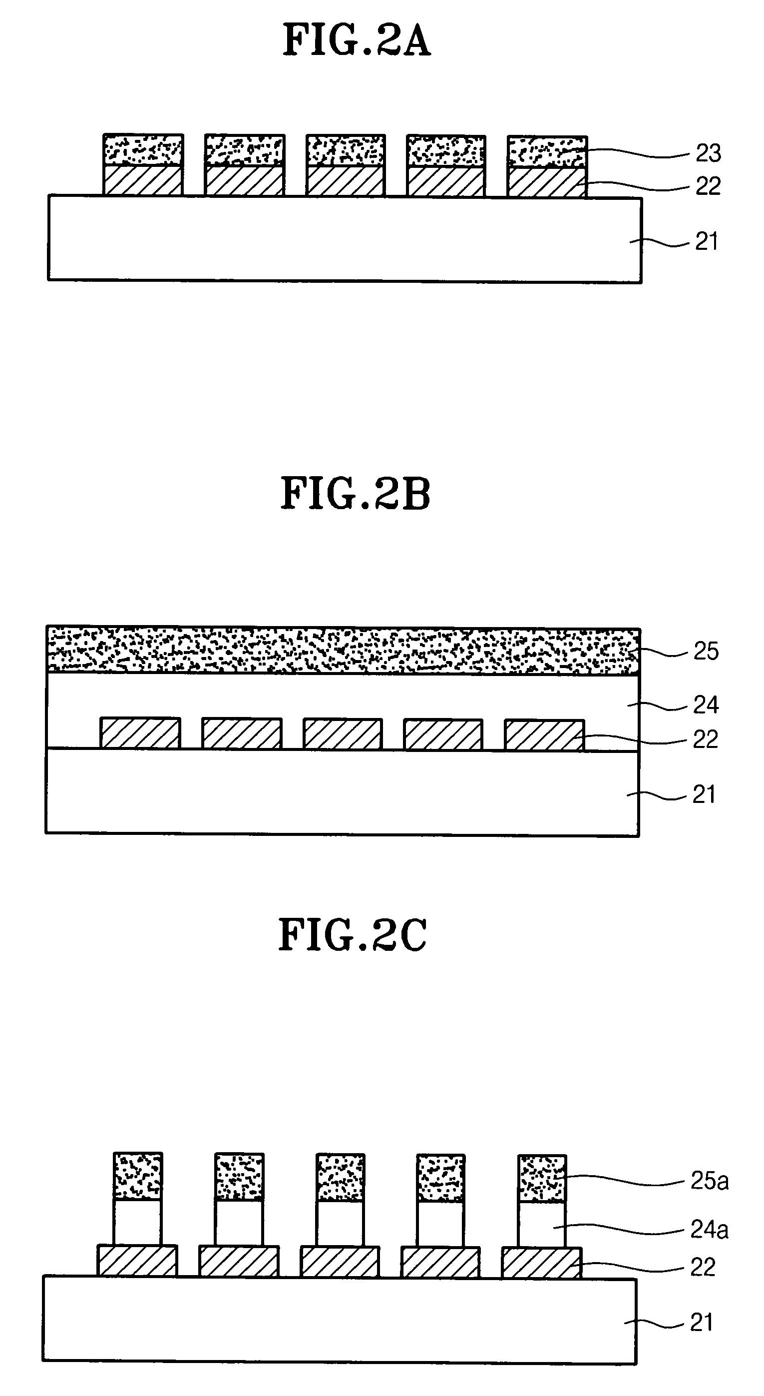
[0034]FIGS. 2A to 2I are the cross-sectional views for illustrating the procedures of manufacturing a phase change RAM device according to an embodiment of the present invention.

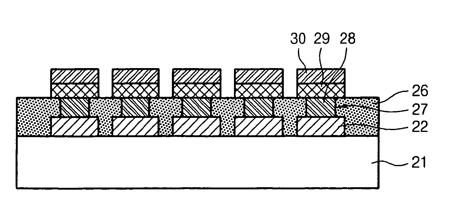
[0035]Referring to FIG. 2A, a plurality of metal pads 22 are formed on the semiconductor substrate 21 by etching a metal layer deposited on the semiconductor substrate 21 using a plurality of mask patterns 23. More specifically, after preparing the semiconductor substrate 21 with an under layer (not shown) including a gate, a tungsten plug, and an interlayer insulating film formed thereon, the metal layer is deposited on the semiconductor substrate 21. After that, the mask patterns 23 are formed on the metal layer, and then the metal layer is etched by using the mask patterns 23, forming a plurality of metal pads 22.

[0036]Referring to FIG. 2B, after removing the mask 23, an oxide layer 24 is formed on the entir...


PUM

PropertyMeasurementUnit
current flowaaaaaaaaaa
sizeaaaaaaaaaa
semiconductoraaaaaaaaaa

Abstract

To effectively lower the current required for changing a phase of a phase change layer in a phase change RAM device, metal pads are formed on a semiconductor substrate, and an oxide layer is formed on the metal pads. Nano-sized copolymer patterns aligned with the metal pads covered by the oxide layer are formed on the oxide layer. The oxide layer is etched to form oxide layer patterns by using the nano-sized copolymer patterns as barrier. The nano-sized copolymer patterns are then removed. A nitride layer is deposited and then etched to expose the oxide layer patterns. The exposed oxide layer patterns are removed to form nano-sized holes exposing the metal pads. Bottom electrodes are then formed in the nano-sized holes. A phase change layer and a top electrode are formed on each of the bottom electrodes.

Description

BACKGROUND OF THE INVENTION[0001]1. Field of the invention[0002]The present invention relates generally to a method of manufacturing a phase change RAM device. More particularly, the present invention relates to a method of manufacturing a phase change RAM device capable of effectively lowering the level of current required for changing a phase of a phase change layer.[0003]2. Description of the Prior Art[0004]In general, the memory devices are mainly classified as (1) random access memory (RAM) devices, which are volatile memory devices that lose information stored therein when power is shut off, and (2) read only memory (ROM) devices, which are non-volatile memory device that retain stored information even if power is shut off. Volatile RAM devices include DRAMs and SRAMs, and non-volatile ROM devices include flash memories, such as an electrically erasable and programmable ROM (EEPROM).[0005]However, although DRAM devices are generally known in the art to be superior memory devic...

Claims


Application Information

Patent Timeline
Patent Type & Authority Patents(United States)
IPC IPC(8): H01L21/06
CPCH01L45/06H01L45/1233H01L45/126H01L45/144H01L45/16H01L45/1675H01L27/2463H10B63/80H10N70/8413H10N70/231H10N70/011H10N70/8828H10N70/063H10N70/826H01L27/10B82Y10/00
Inventor CHANG, HEON YONGPARK, HAE CHANHONG, SUK KYOUNG
Owner SK HYNIX INC
Why Eureka
Try Eureka