Supercharge Your Innovation With Domain-Expert AI Agents!

Scribing tool and method

a technology of scribing tool and semiconductor wafer, which is applied in the direction of manufacturing tools, writing aids, paper/cardboard containers, etc., can solve the problems of preventing the mechanism from operating properly, the use of saws to dice wafers has proved unsatisfactory, and the diamond tips of the machine would wear down quickly, so as to maintain the pressure on the semiconductor wafer

Inactive Publication Date: 2008-07-01
MICRO PROCESSING TECH
View PDF14 Cites 16 Cited by
  • Summary
  • Abstract
  • Description
  • Claims
  • Application Information

AI Technical Summary

Benefits of technology

"The invention is a new scribing tool and method for semiconductor wafer scribing that improves tool life while maintaining the benefits of scribing over sawing in certain applications. The scribing tool includes a yoke with yoke legs that support a semiconductor wafer scribing wheel for rotation and sideways deflection resistance during use. The method involves positioning the scribing tool above the semiconductor wafer and engaging the scribing wheel with the wafer to exert pressure and form scribe lines. The technical effects include improved tool life, reduced costs, and improved efficiency in semiconductor wafer scribing."

Problems solved by technology

Problems were observed with these scribe machines when hard semiconductor materials such as silicon were scribed.
The diamond tips used in the machines would wear down quickly and have to be changed frequently at some expense.
In certain new types of semiconductor devices made out of silicon materials, the use of saws to dice wafers has proven to be unsatisfactory.
In MEMS devices, the debris created by the sawing processing can prevent the mechanisms from operating properly.
In very thin integrated circuits, such as those used in smart cards, the protruding diamond particles in the blade can cause chipping and fracturing of the device die.
While this approach solved the problem with debris and reduced chipping and fracturing, short diamond tool life when scribing a hard material like silicon is still a problem.

Method used


Image

  • Scribing tool and method
  • Scribing tool and method
  • Scribing tool and method

Examples


Embodiment Construction

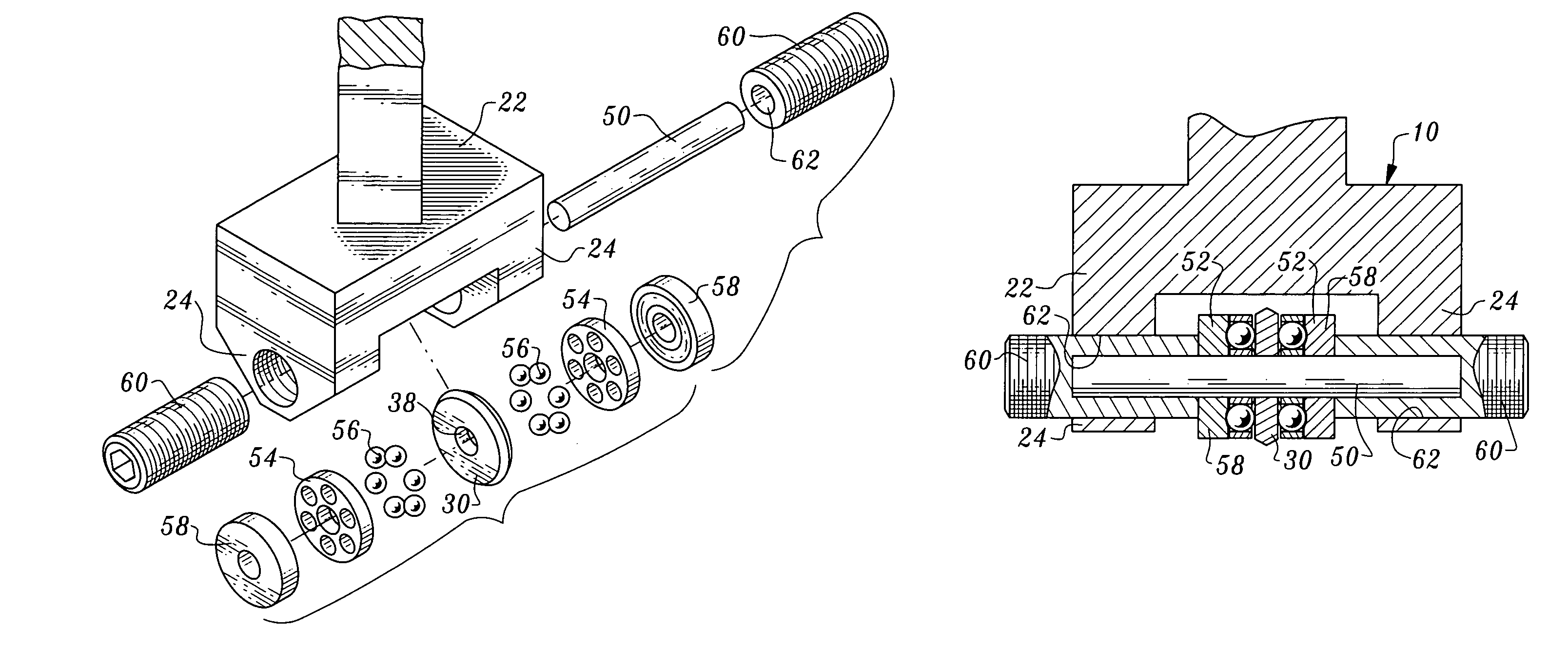
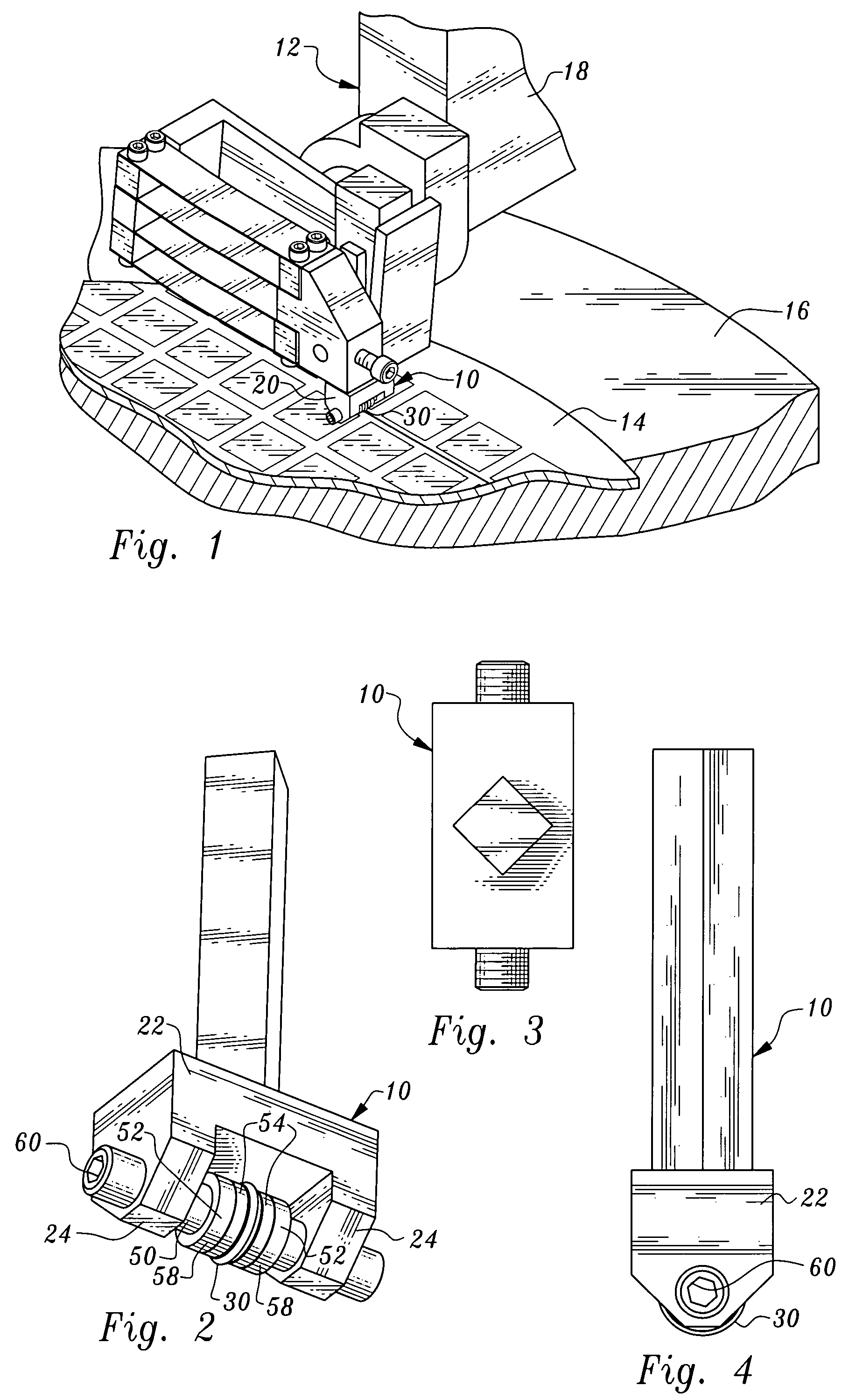
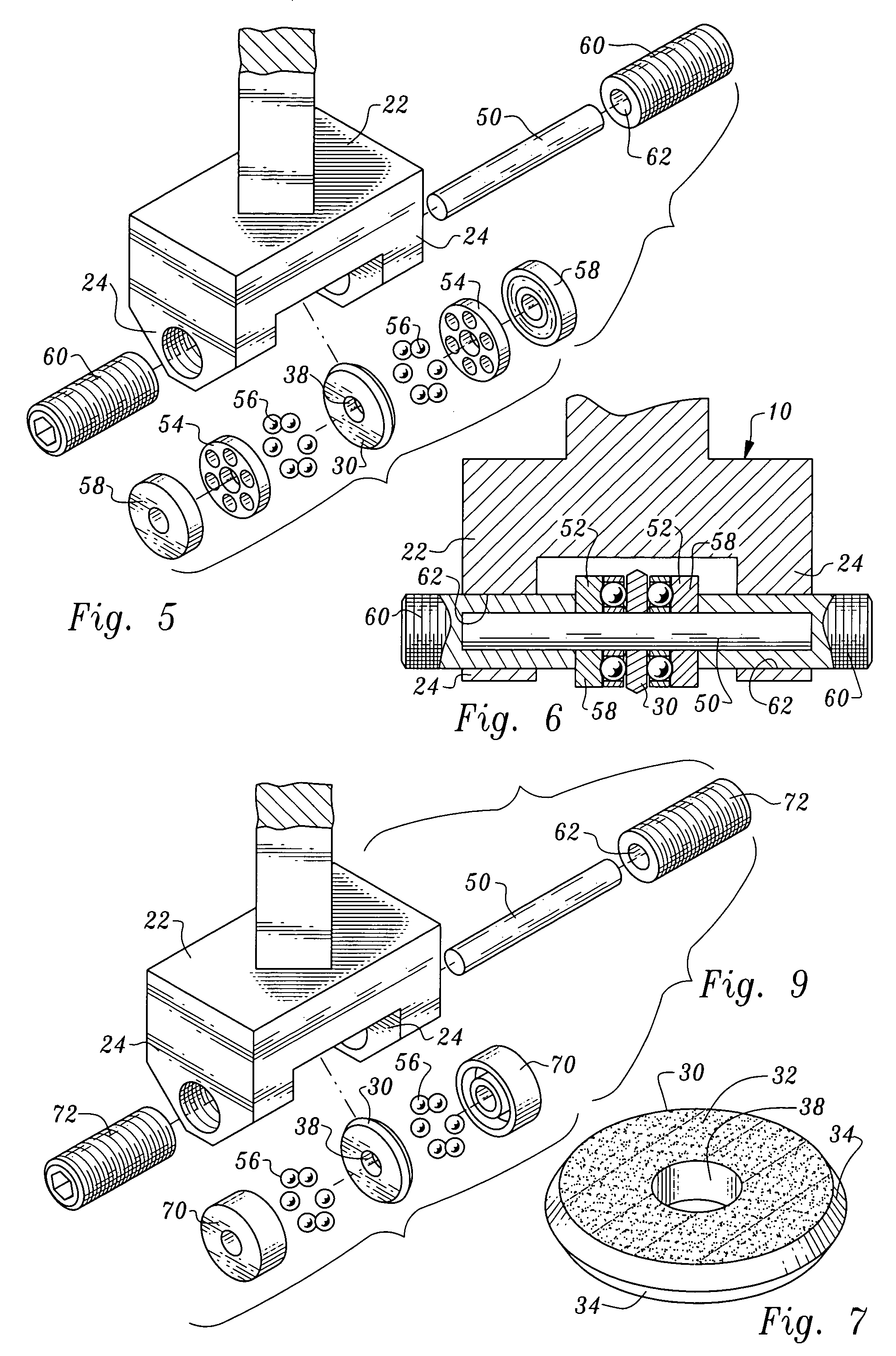
[0030]FIGS. 1-8 illustrate a scribing tool constructed in accordance with the teachings of the present invention. The scribing tool is designated by reference numeral 10 and in FIG. 1 the scribing tool is shown employed in a semiconductor scribing apparatus 12 for dicing semiconductor wafers. One such wafer, semiconductor wafer 14, is illustrated. The wafer is located on a support 16.

[0031]Co-pending U.S. patent application Ser. No. 10 / 462,398, filed Jun. 16, 2003, discloses a scribe tool supported by a multi-stage gantry, the multi-stage gantry operable to selectively bring the scribe tool into engagement with the wafer and to move the scribe tool relative to the wafer while in engagement therewith to form a scribe line in the wafer.

[0032]The arrangement shown in FIG. 1 incorporates such a multi-stage gantry, the latter identified by reference numeral 18. It is to be appreciated, however, that the tool of the present invention may be utilized and the method of the present invention...


PUM

PropertyMeasurementUnit
widthaaaaaaaaaa
thicknessaaaaaaaaaa
diameteraaaaaaaaaa

Abstract

A scribing tool for use in semiconductor scribing apparatus includes a rotatable semiconductor wafer scribing wheel engageable with the semiconductor wafer to form a scribe line when the tool exerts pressure on the semiconductor wafer and the scribing wheel rotates. Bearings are engageable with the scribing wheel sides to resist sideways deflection during the scribing operation.

Description

TECHNICAL FIELD[0001]This invention relates to the manufacture of semiconductor devices and circuits and more particularly to a tool and method for scribing semiconductor wafers.BACKGROUND OF THE INVENTION[0002]In the very early days of semiconductor device fabrication, the individual devices were separated from the other devices fabricated on the wafer by using the dicing process of scribing and breaking. The scribing process was carried out using a sharp-tipped diamond tool and initially done by hand. Later, automatic scribing machines such as those described in U.S. Pat. Nos. 3,094,785 and 5,820,006 were developed. These scribing machines provided a way to precisely position the diamond scribe tip as it traversed the width of the wafer and created the scribe line. This is necessary because the scribe line must stay within the scribe street that can be as narrow as 50 microns in width. Problems were observed with these scribe machines when hard semiconductor materials such as sili...

Claims


Application Information

Patent Timeline
Patent Type & Authority Patents(United States)
IPC IPC(8): B26D3/08
CPCB26D3/085B27B5/30B27B5/32B28D5/022H01L21/67092B28D1/225H01L21/78Y10T83/0385Y10T83/0333Y10T83/0341
Inventor LINDSEY, JR., PAUL C.LINDSEY, CHRISTOPHER K.ATKINSON, JEFFERY D.
Owner MICRO PROCESSING TECH
Features
  • R&D
  • Intellectual Property
  • Life Sciences
  • Materials
  • Tech Scout
  • Unparalleled Data Quality
  • Higher Quality Content
  • 60% Fewer Hallucinations
Learn More