
Light emitting device
a technology of light-emitting devices and transparent electrodes, which is applied in the manufacture of electric discharge tubes/lamps, discharge tubes luminescent screens, electrode systems, etc., can solve the problems of uneven distribution of intra-plane electric potentials, high film resistance of transparent electrodes, and fluctuation of luminance, so as to reduce the thickness of transparent electrodes, high film resistance, and the effect of film resistan
- Summary
- Abstract
- Description
- Claims
- Application Information
AI Technical Summary
Benefits of technology
Problems solved by technology
Method used
Image

Examples
embodiment mode 1
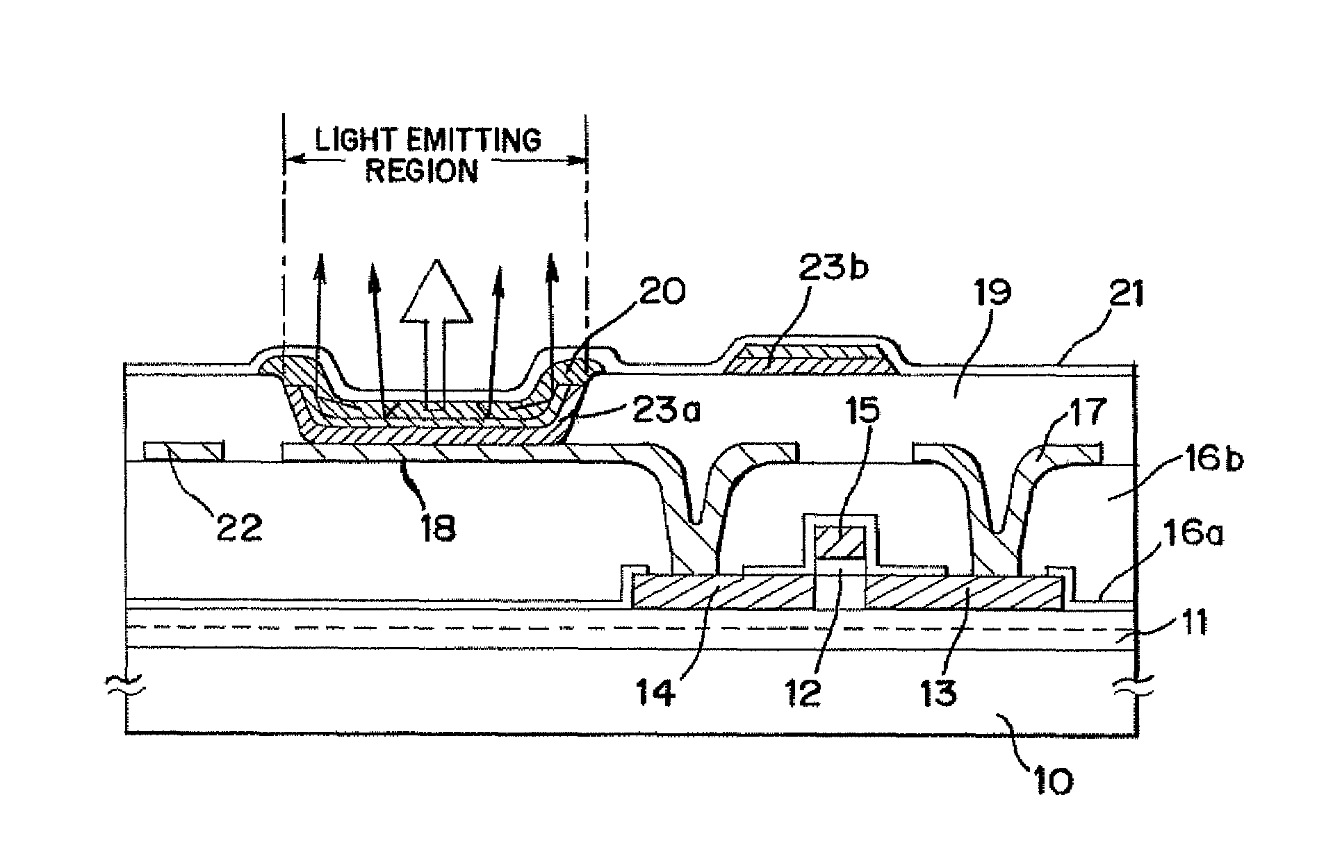
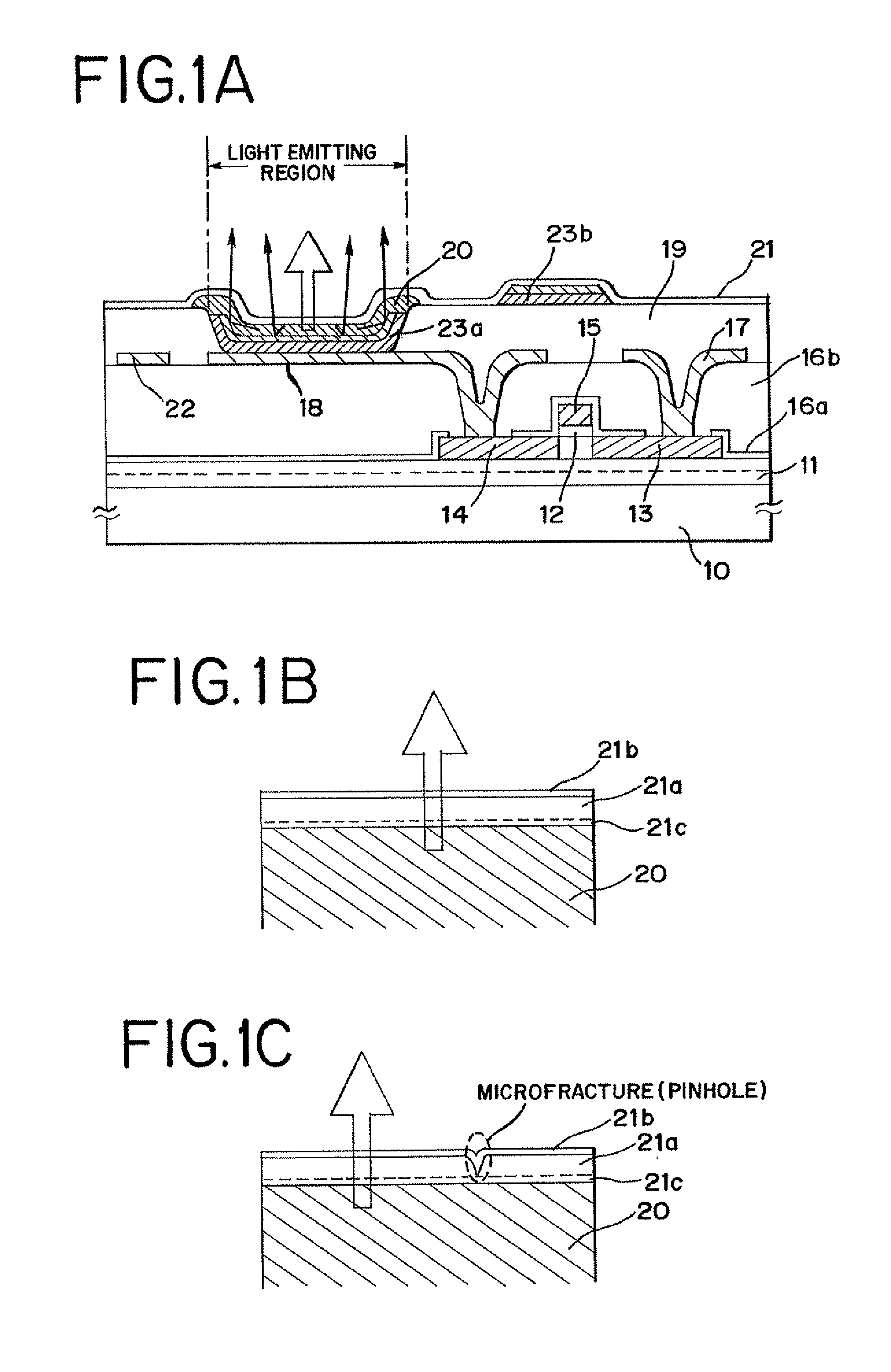
[0067]FIG. 1A is a cross-sectional view of an active matrix light emitting device (a part of one pixel). Described here as an example is a light emitting element which uses as its light emitting layer a light emitting layer comprising an organic material formed of a high molecular weight material that emits white light.
[0068]In FIG. 1A, a TFT (p-channel TFT) on a substrate 10 having an insulating surface is an element for controlling a current flowing into an EL layer (organic compound-containing layer) 20 that emits white light. Of regions denoted by 13 and 14, one is a source region and the other is a drain region. A base insulating film 11 (here, a laminate of an insulating nitride film as a lower layer and an insulating oxide film as an upper layer) is formed on the substrate 10. A gate insulating film 12 is placed between a gate electrode 15 and an active layer of the TFT.
[0069]For a substrate 10 having an insulating surface, a glass substrate, a quartz substrate, and a plastic...
embodiment mode 2
[0090]A method of combining a white color luminescent element and a color filter (hereinafter, referred to as color filter method) will be explained in reference to FIG. 5A as follows.
[0091]The color filter method is a system of forming a light emitting element having a light emitting layer comprising an organic material displaying white color luminescence and passing the provided white color luminescence through a color filter to thereby achieve luminescence of red, green, and blue.
[0092]Although there are various methods of achieving white color luminescence, a case of using a luminescent layer comprising a high molecular material formable by application will be explained here. In this case, doping of a color pigment to the high molecular material for constituting a luminescent layer can be carried out by preparing a solution and can extremely easily be achieved in comparison with a vapor deposition method for carrying out common vapor deposition for doping a plurality of color pi...
embodiment mode 3
[0106]Here, a total of an EL module and arrangement of a drying agent will be explained in reference to FIGS. 4A and 4B. FIG. 4A is a top surface view of the EL module. FIG. 4B is a part of a cross-sectional view.
[0107]A substrate provided with numerous TFTs (also referred to as TFT substrate) is provided with a pixel portion 40 for display, driver circuits 41a and 41b for driving respective pixels of the pixel portion, a connecting portion for connecting the electrode provided over the EL layer and an extended wiring, a terminal portion 42 for pasting FPC for connecting to outside circuit and a drying agent 44. Further, in FIG. 4A and FIG. 4B, the drying agent 44 may be arranged to overlap a portion of the driver circuits, however, the drying agent can also be arranged such that a total of the driver circuits is concealed by the drying agent 44 as shown in FIG. 4C. Further, the constitution is hermetically sealed by the substrate for sealing the EL element and a seal member 49. Fur...
PUM
 Abstract
Description
Claims
Application Information