Biasing scheme for large format CMOS active pixel sensors

a technology of cmos active pixel and bias scheme, which is applied in the field of active pixel sensor arrays, can solve the problems of increasing image quality degradation at low illumination, giving rise to fixed pattern noise (fpn) in the array, and affecting the quality of image, so as to achieve reliable hard or soft reset operation of the pixel cell, and the effect of reducing the noise on the vaa

Active Publication Date: 2008-08-05
MICRON TECH INC
View PDF6 Cites 8 Cited by
  • Summary
  • Abstract
  • Description
  • Claims
  • Application Information

AI Technical Summary

Benefits of technology

[0030]In another exemplary embodiment, a transistor is placed between the line VAA<sub2>—< / sub2>PIX and the column line VAA<sub2>—< / sub2>PIX<sub2>—< / sub2>COL. By making the transistor, preferably an n-MOS transistor, operate in its saturation region, noise on the VAA<sub2>—< / sub2>PIX line can be filtered out. Further, by adding a p-MOS transistor in parallel with the n-MOS transistor, a more reliable hard or soft reset operation of the pixel cell can be obtained.

Problems solved by technology

Vth represents a deviation of the effective threshold voltage, which gives rise to fixed pattern noise (FPN) in the array.
FPN increases with illumination, but causes more degradation in image quality at low illumination.
CMOS (APS) sensors have higher FPN than charge-coupled devices (CCDs) and suffer from column FPN, which may appear as shadow stripes in the image and can result in image quality degradation.
A problem arises, however, during the reset operation.
If a large format array is built based on the architecture shown in FIG. 1, a problem associated with the hard reset occurs due to the voltage (I·R) drops along the VAA—PIX line.
In addition, if the VAA—PIX line is contaminated by noise, that noise is sampled on a photodiode.

Method used


Image

  • Biasing scheme for large format CMOS active pixel sensors
  • Biasing scheme for large format CMOS active pixel sensors
  • Biasing scheme for large format CMOS active pixel sensors

Examples


Embodiment Construction

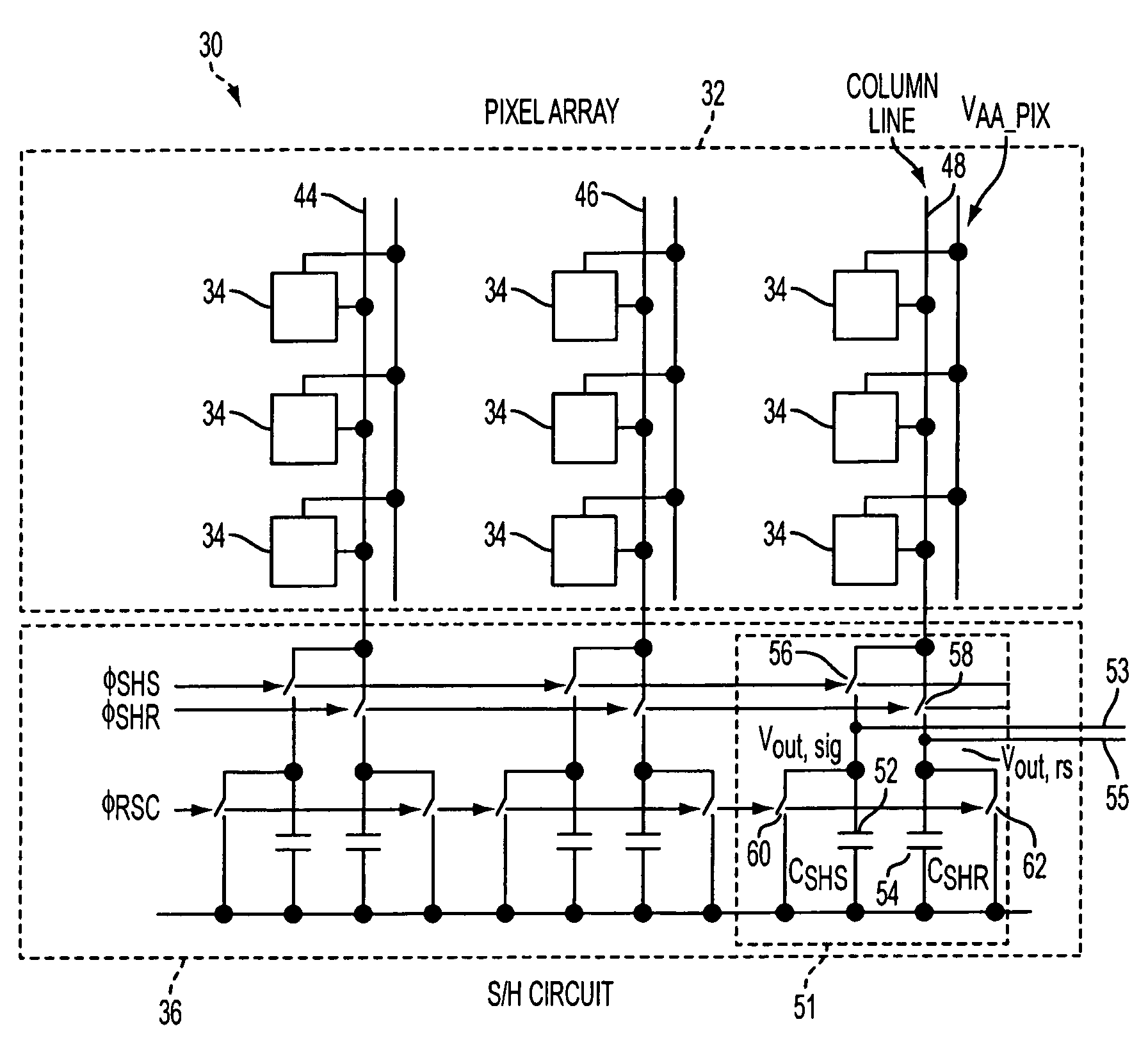
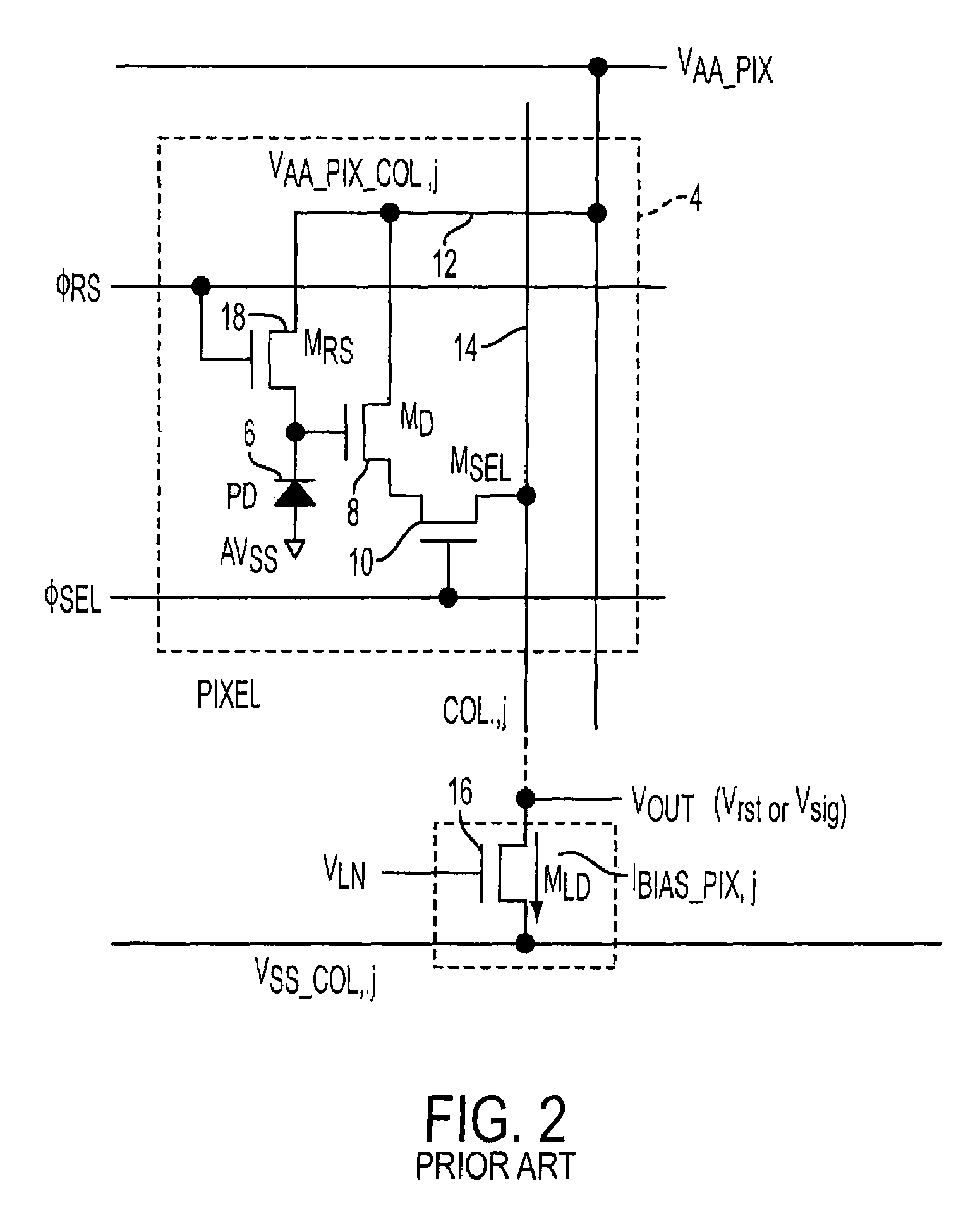
[0049]Referring initially to FIG. 7, an APS 30 according to an exemplary embodiment of the present invention is shown. APS 30 includes a number of pixels 34 arranged in an array 32. Pixels 34 may employ many different architectures, including the 3 transistor (3T) architecture shown in FIG. 2 or 4 transistor (4T) or higher order transistor architectures known in the art. APS 30 does not use the FIG. 2 current sink transistor 16, but rather employs a capacitor loaded source follower formed by connecting the column lines 44, 46, 48 of the array to sample and hold circuit 36 in the manner shown in FIG. 7. Consequently, the load transistor 16 of FIG. 2 is eliminated from the circuit. For clarity, certain features of APS 30 not critical to the invention have been eliminated in the drawing of FIG. 7.

[0050]Column read-out circuitry of this embodiment will be described for column 48 as being representative of other columns in the array. Connected to column line 48 is a read-out circuit 51 p...


PUM


Abstract

An image sensor includes circuitry compensating for voltage drops in a VSS line. The image sensor includes a plurality of photoreceptors arranged in a pixel array having a number of column lines, and read-out circuitry on the column lines. The read-out circuitry provides substantially equal currents on each column line so as to compensate for voltage drops in the VSS line and provide more accurate pixel signals. The image sensor also includes circuitry for filtering noise from a voltage supply line, and for providing hard and / or soft reset operations.

Description

BACKGROUND OF THE INVENTION[0001]1. Field of the Invention[0002]The invention relates to active pixel sensor arrays and, more particularly, to a biasing arrangement for complementary metal oxide semiconductor (CMOS) active pixel sensor arrays.[0003]2. Description of the Related Art[0004]Active pixel sensor (APS) imaging devices are described in U.S. Pat. No. 5,471,515, for example. APS imaging devices include an array of pixel cells, generally arranged in rows and columns. Each pixel cell includes a photodetector (e.g., photodiode) that converts light energy into electric signals. The pixel cell also includes one or more transistors. The transistors typically provide amplification, read-out control, and reset of the photodetector signal, and operate to provide reset signal and a photodetector pixel signal as output signals from the pixel cell.[0005]The architecture of a conventional imaging device with a CMOS APS 2 is illustrated in FIGS. 1 and 2. APS 2 includes a row and column arr...

Claims


Application Information

Patent Timeline
Patent Type & Authority Patents(United States)
IPC IPC(8): H04N3/14H04N5/335H04N5/217G09G3/20H04N5/359H04N5/374H04N5/378
CPCH04N3/1568H04N5/3575H04N5/378H04N5/3745H04N5/3658H04N25/616H04N25/671H04N25/677H04N25/77H04N25/75
Inventor NAKAMURA, JUNICHITAKAYANAGI, ISAO
Owner MICRON TECH INC
Why Eureka
Try Eureka