

Method for verifying performance of an array by simulating operation of edge cells in a full array model
a full array model and array technology, applied in the field of array modeling methods and software, can solve the problems of loading effects and the inability to compute the operation within the cell, and achieve the effect of reducing computation tim
- Summary
- Abstract
- Description
- Claims
- Application Information
AI Technical Summary
Benefits of technology
Problems solved by technology
Method used
Image

Examples
Embodiment Construction
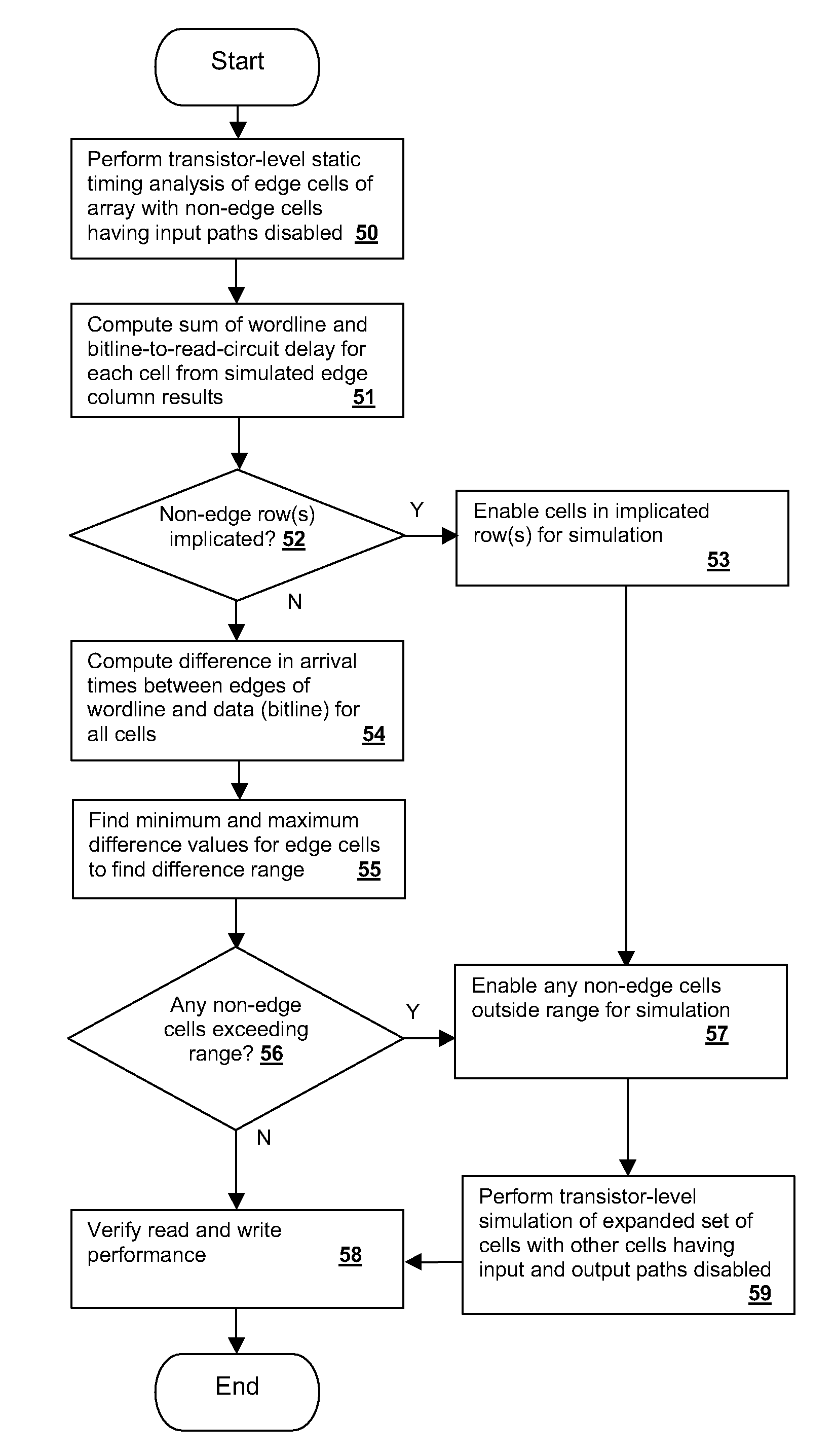
[0021]The present invention concerns a computer-performed design verification method and computer program for carrying out the method. The program may be a dedicated program having program instructions in accordance with an embodiment of the present invention, or an existing design tool such as one of the variety of programs, such as “Simulation Program with Integrated Circuits Emphasis” (SPICE—originally a development of the University of California, Berkeley) can be employed. The particular simulation program must be modified or include specific operation directed as detailed herein below by accepting simulation input directives that can logically disable devices within a cell. The simulation results may then be used to provide input to a static timing analysis tool such as EINSTIMER (a product of International Business Machines Corporation).
[0022]The method of the present invention dramatically reduces the amount of time to perform a full circuit level verification of array read ...
PUM
 Abstract
Description
Claims
Application Information