Method of manufacturing a semiconductor integrated circuit, a program for a computer automated design system, and a semiconductor integrated circuit

a semiconductor integrated circuit and integrated circuit technology, applied in the field of semiconductor integrated circuits, can solve the problems of failure of connection, more difficult to form wiring shapes for the connection of elements as designed, and more difficult to bury via plugs in the via hol

Inactive Publication Date: 2008-09-09
KK TOSHIBA
View PDF2 Cites 122 Cited by
  • Summary
  • Abstract
  • Description
  • Claims
  • Application Information

AI Technical Summary

Problems solved by technology

With movement toward further miniaturization of a semiconductor integrated circuit, it has become more difficult to form wiring shapes for the connection of elements as designed.
As a result, a phenomenon (shortening) occurs in which the wiring does not reach a position of a via hole, thereby causing a connection failure.
An increase of an aspect ratio of a via has also been advanced by the requirement for miniaturization of the wiring, and it has become more difficult to bury a via plug in the via hole.
As a result, it becomes difficult to increase the density of the circuit, causing an increase of chip size.

Method used


Image

  • Method of manufacturing a semiconductor integrated circuit, a program for a computer automated design system, and a semiconductor integrated circuit
  • Method of manufacturing a semiconductor integrated circuit, a program for a computer automated design system, and a semiconductor integrated circuit
  • Method of manufacturing a semiconductor integrated circuit, a program for a computer automated design system, and a semiconductor integrated circuit

Examples


Embodiment Construction

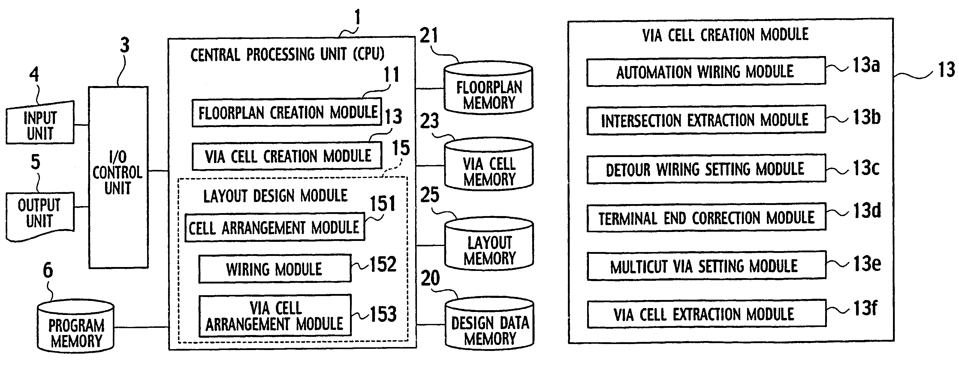
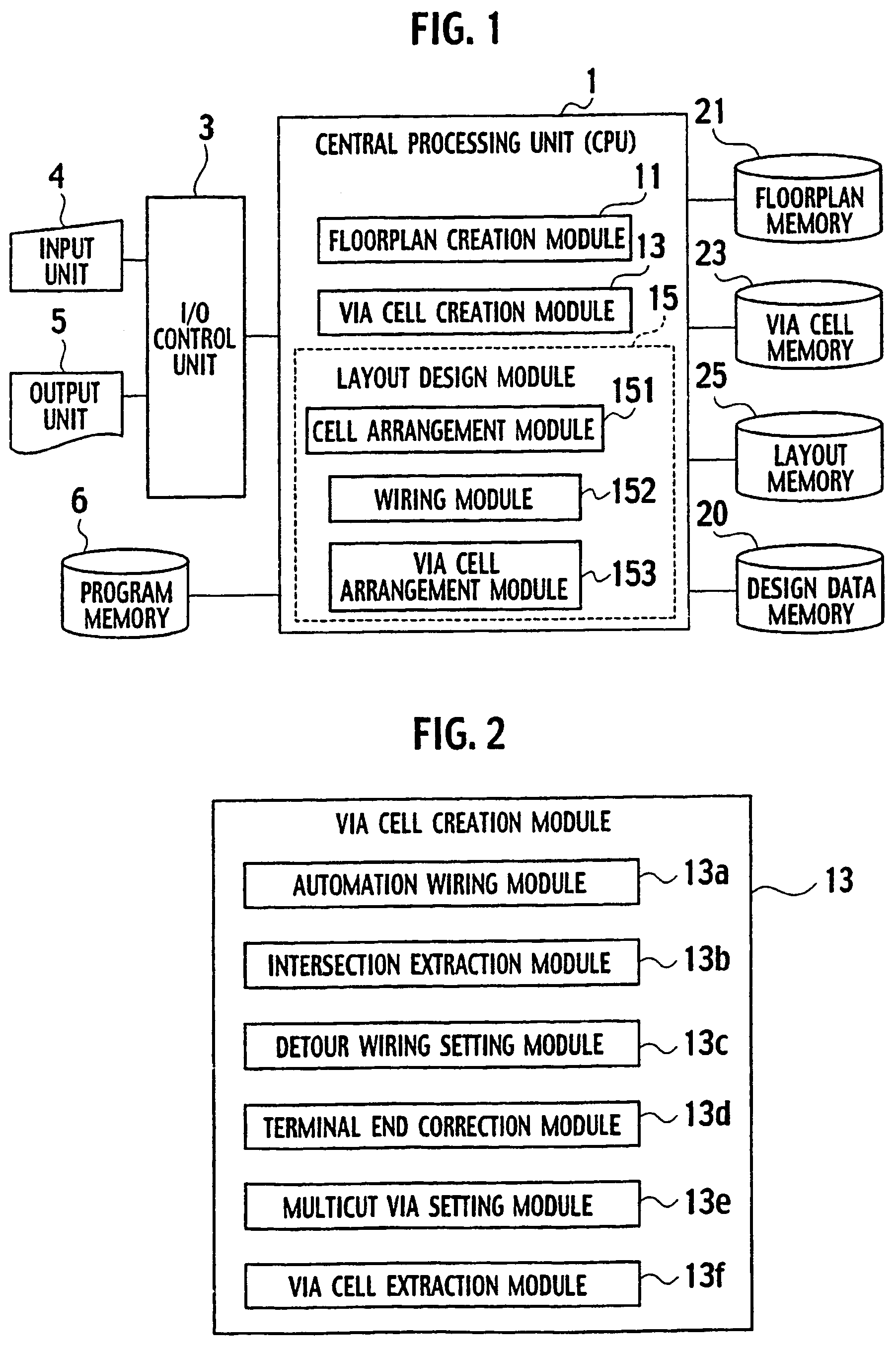
[0034]Various embodiments of the present invention will be described with reference to the accompanying drawings. It is to be noted that the same or similar reference numerals are applied to the same or similar parts and elements throughout the drawings, and the description of the same or similar parts and elements will be omitted or simplified. In the following descriptions, numerous details are set forth such as specific signal values, etc. to provide a thorough understanding of the present invention. However, it will be obvious to those skilled in the art that the present invention may be practiced without such specific details.

[0035]As shown in FIG. 1, a design system according to an embodiment of the present invention includes a central processing unit (CPU) 1, which executes various arithmetic operations for a layout design and the like, an input and output control unit 3 connected to the CPU 1, an input unit 4 which inputs information such as data or instructions from an oper...


PUM


Abstract

A method for manufacturing a semiconductor integrated circuit uses layout data designed by a sequence of processes. The sequence of processes includes disposing a lower-layer wiring pattern on an imaginary lower-layer wiring layer and an upper-layer wiring pattern perpendicular to the lower-layer wiring pattern on an imaginary upper-layer wiring layer implemented in the graphics image space, providing a detour pattern including a first detour pattern connected to the upper-layer wiring pattern, providing a plurality of via patterns connecting the lower-layer and upper-layer wiring patterns, and forming a via cell pattern.

Description

CROSS REFERENCE TO RELATED APPLICATIONS AND INCORPORATION BY REFERENCE[0001]This application is based upon and claims the benefit of priority from the prior Japanese Patent Applications No. P2005-041158, filed on Feb. 17, 2005, the entire contents of which are incorporated herein by reference.BACKGROUND OF THE INVENTION[0002]1. Field of the Invention[0003]The present invention relates to a semiconductor integrated circuit and, more specifically, to a semiconductor integrated circuit and a method of manufacturing a semiconductor integrated circuit including a plurality of metal layers connected with a plurality of vias.[0004]2. Description of the Related Art[0005]With movement toward further miniaturization of a semiconductor integrated circuit, it has become more difficult to form wiring shapes for the connection of elements as designed. In particular, in an advanced semiconductor integrated circuit including a multi-layer interconnection, a terminal end of a wiring in one layer in ...

Claims


Application Information

Patent Timeline
Patent Type & Authority Patents(United States)
IPC IPC(8): G06F17/50
CPCH01L21/76838
Inventor TAMURA, NAOYUKIURAKAWA, YUKIHIRO
Owner KK TOSHIBA
Why Eureka
Try Eureka