Electronic device and a process for forming the electronic device

a technology of electronic devices and diodes, applied in the direction of diodes, semiconductor devices, electrical apparatus, etc., can solve the problem of insufficient control of junctions within the diodes structur

Active Publication Date: 2008-10-07
TAIWAN SEMICON MFG CO LTD
View PDF36 Cites 15 Cited by
  • Summary
  • Abstract
  • Description
  • Claims
  • Application Information

AI Technical Summary

Problems solved by technology

Having no gate electrode or having just a single signal line for the gate electrode(s) may result in insufficient control over a junction within the diode structure when operated under different conditions.

Method used


Image

  • Electronic device and a process for forming the electronic device
  • Electronic device and a process for forming the electronic device
  • Electronic device and a process for forming the electronic device

Examples


Embodiment Construction

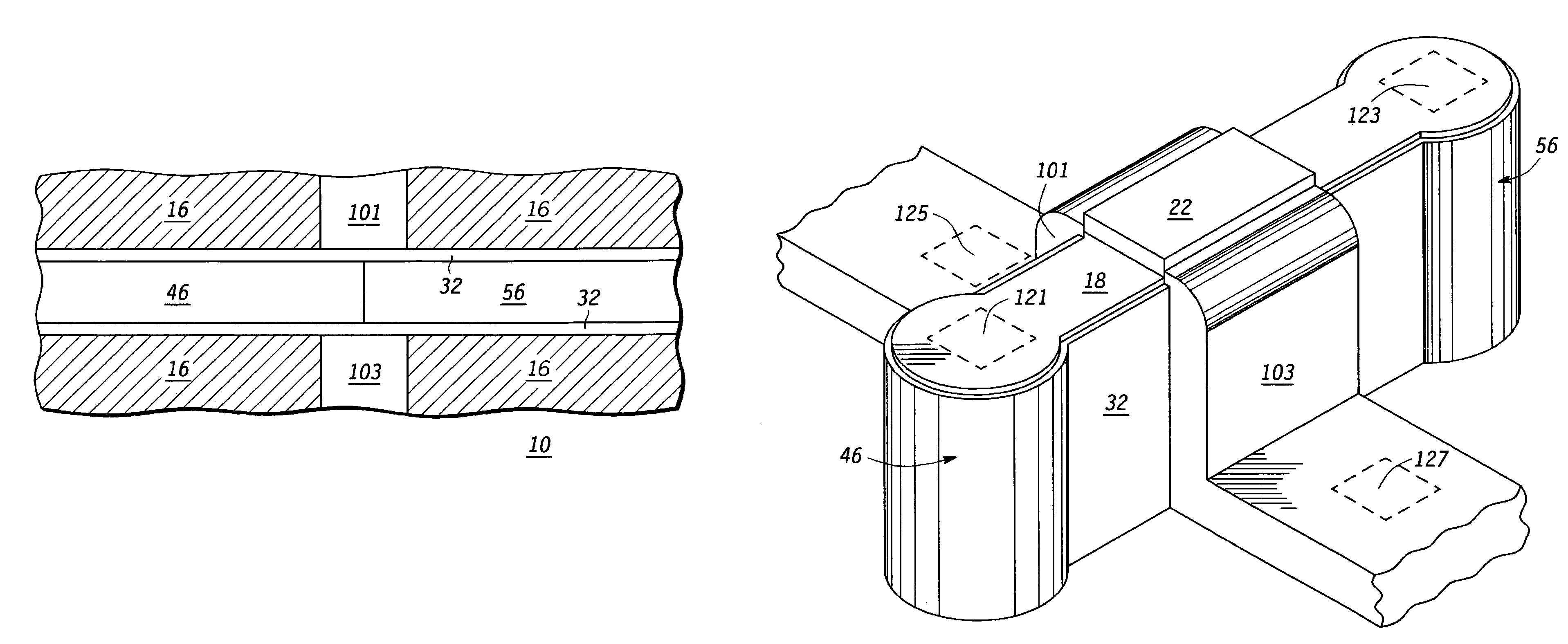
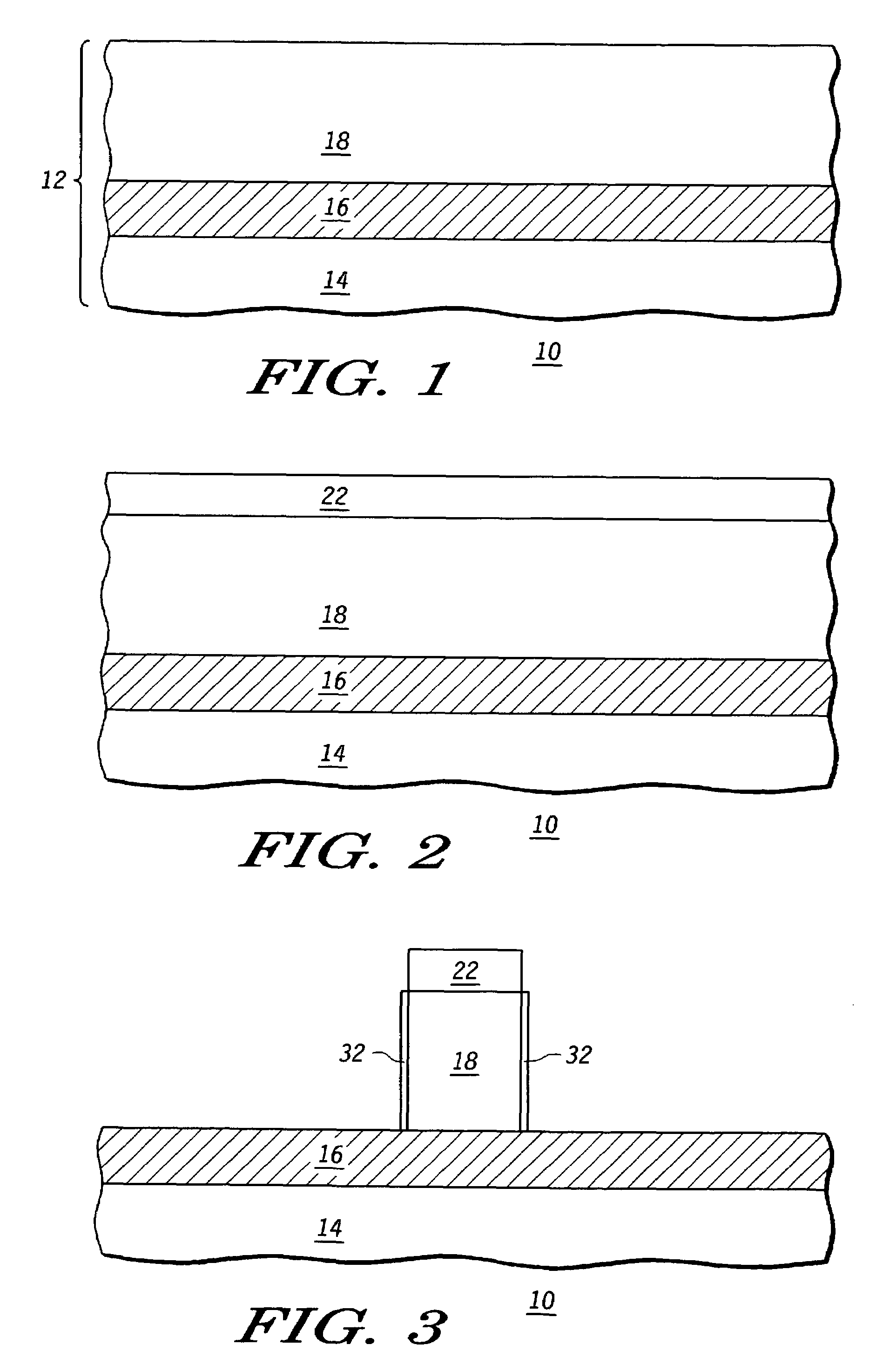
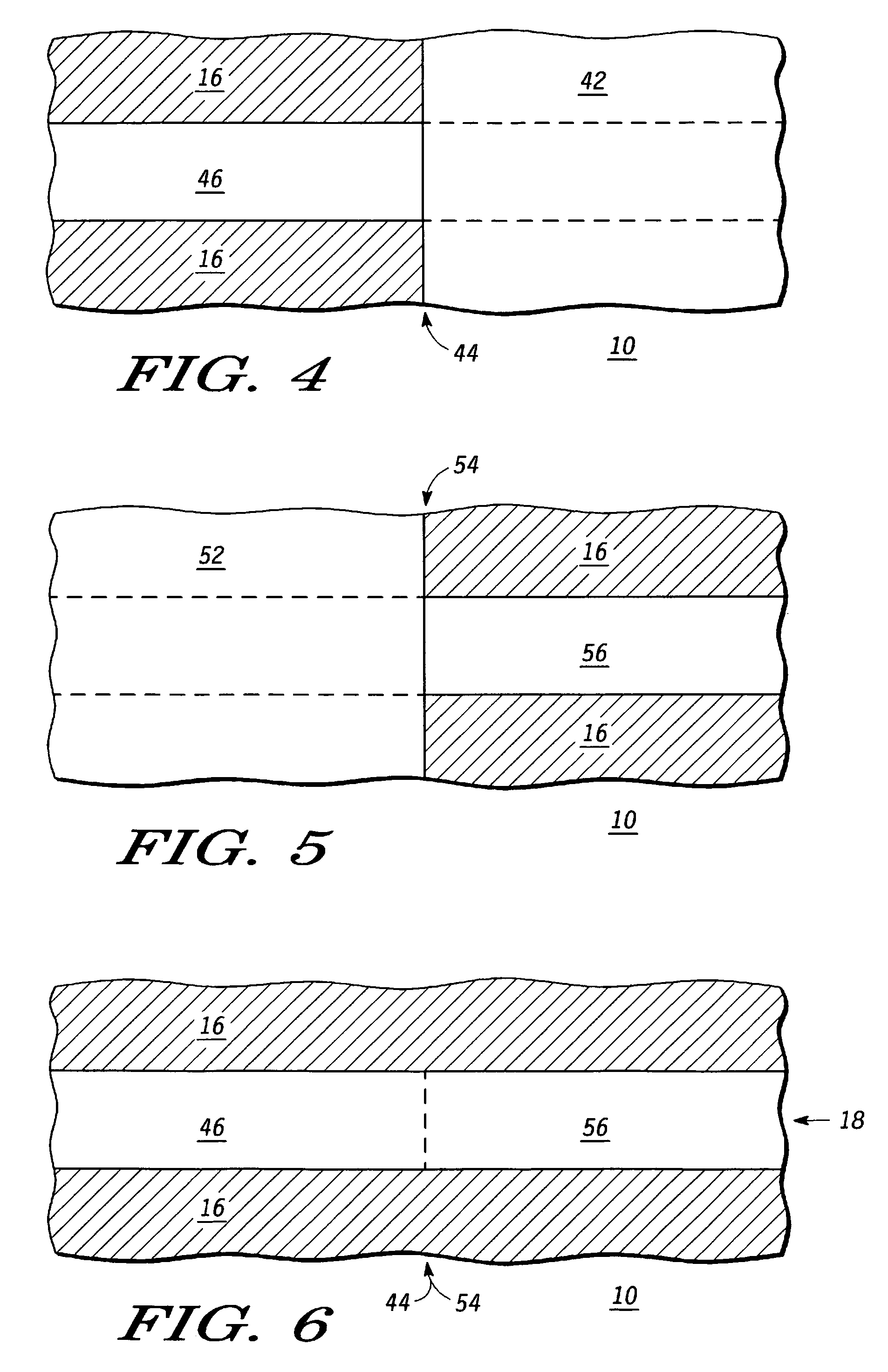
[0023]An electronic device can include a gated diode that can be formed and have more than one independently controlled gate electrode to allow for more control options of the gated diode. In a particular embodiment, the gated diode can have substantially uniform current flow across the entire cross-section of the structure. In a particular embodiment, the gated diode can have improved current carrying capability, lower parasitic capacitive coupling than a conventional gated diode, or any combination thereof. Particular, non-limiting embodiments will be better understood with reference to FIGS. 1 through 19.

[0024]Some terms are defined or clarified as to their intended meaning as they are used within this specification. As used herein the term “lightly doped” is intended to mean in a range of approximately 1 E15 to approximately 1 E18 atoms per cm3. Also the term “heavily doped” is intended to mean a dopant concentration in a range of approximately 1 E19 to approximately 1 E22 atoms...


PUM


Abstract

An electronic device can include a gated diode, wherein the gated diode includes a junction diode structure including a junction. A first conductive member spaced apart from and adjacent to the junction can be connected to a first signal line. A second conductive member, spaced apart from and adjacent to the junction, can be both electrically connected to a second signal line and electrically insulated from the first conductive member. The junction diode structure can include a p-n or a p-i-n junction. A process for forming the electronic device is also described.

Description

BACKGROUND[0001]1. Field of the Disclosure[0002]The present disclosure relates to electronic devices, more particularly, to gated diode structures and processes for forming them.[0003]2. Description of the Related Art[0004]A diode structure is among the simplest of electronic components and can be used in many applications. A diode structure may or may not be gated. When gated, a single signal line can be used to control one or more gate electrodes of the diode structure. Having no gate electrode or having just a single signal line for the gate electrode(s) may result in insufficient control over a junction within the diode structure when operated under different conditions.BRIEF DESCRIPTION OF THE DRAWINGS[0005]The present disclosure may be better understood, and its features and benefits made apparent to those skilled in the art by referencing the accompanying drawings. The subject of the disclosure is illustrated by way of example and not limitation in the accompanying figures.[0...

Claims


Application Information

Patent Timeline
Patent Type & Authority Patents(United States)
IPC IPC(8): H01L21/00H01L21/20H01L21/36H01L21/84
CPCH01L27/0811H01L29/0657H01L29/42312H01L29/7391H01L29/785Y02E10/548
Inventor MATHEW, LEOKHAZHINSKY, MICHAEL G.
Owner TAIWAN SEMICON MFG CO LTD
Why Eureka
Try Eureka