Semiconductor device

a technology of semiconductor devices and side walls, applied in semiconductor devices, semiconductor/solid-state device details, coatings, etc., can solve problems such as local insufficient filling, and achieve the effects of increasing bonding strength, increasing cross section of first walls, and increasing bonding strength between the first wall and the side wall of the housing

Active Publication Date: 2008-10-07
NICHIA CORP
View PDF16 Cites 59 Cited by
  • Summary
  • Abstract
  • Description
  • Claims
  • Application Information

AI Technical Summary

Benefits of technology

[0014]With the background described above, an object of the present invention is to provide a semiconductor device wherein the adhesive components do not overflow nor leak to the wire bonding area even when an adhesive consisting of adhesive components having low surface tension is used in the adhesive layer for die bonding, and the overflow and leak preventing function can be maintained satisfactorily even when the device is made smaller and thinner.

Problems solved by technology

The first wall is small in height to such an extent that does not hamper wire bonding, and therefore it is difficult to fill in the molding material which may result in locally insufficient filling in case the molding material has high viscosity.

Method used


Image

  • Semiconductor device
  • Semiconductor device
  • Semiconductor device

Examples


first embodiment

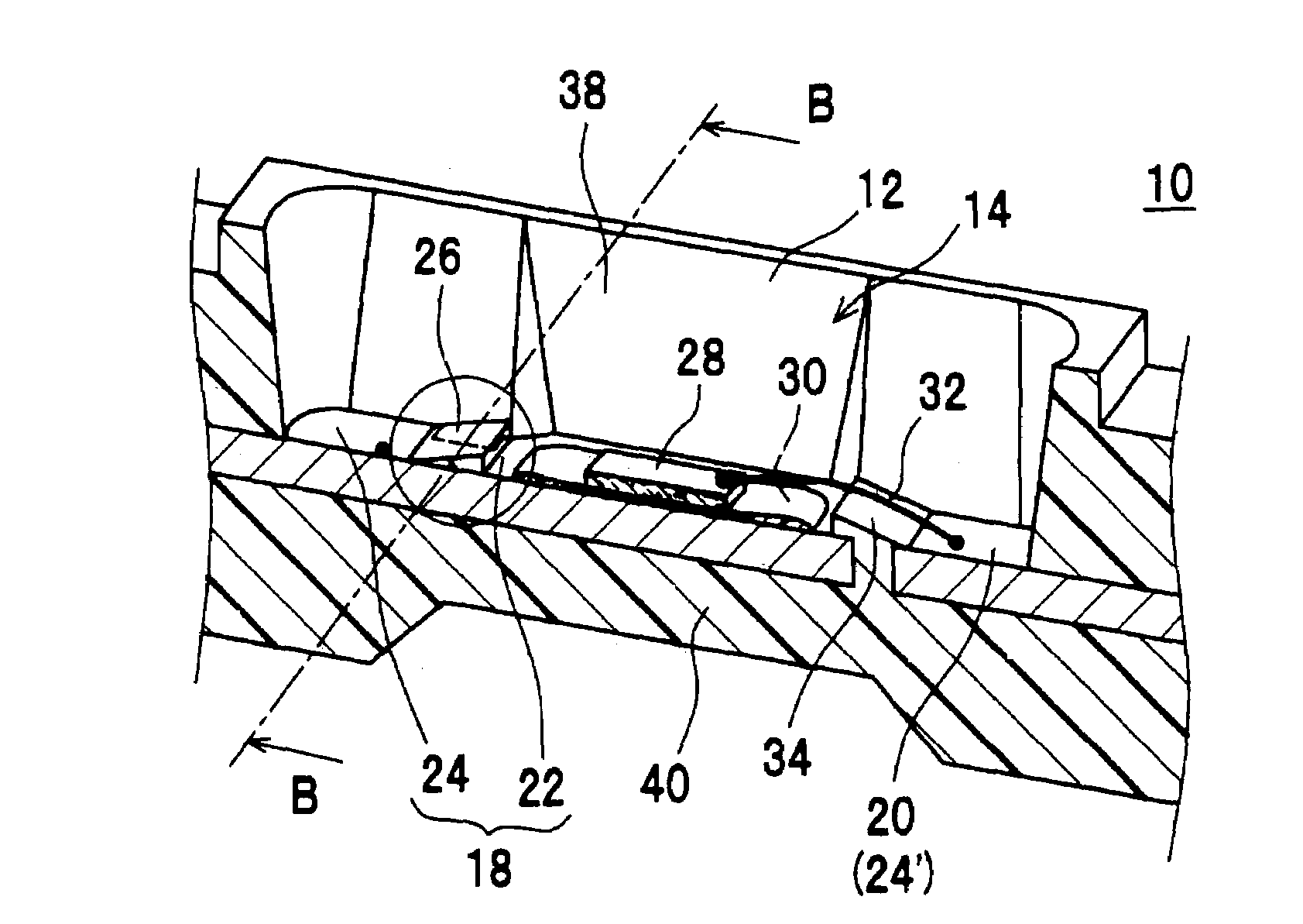
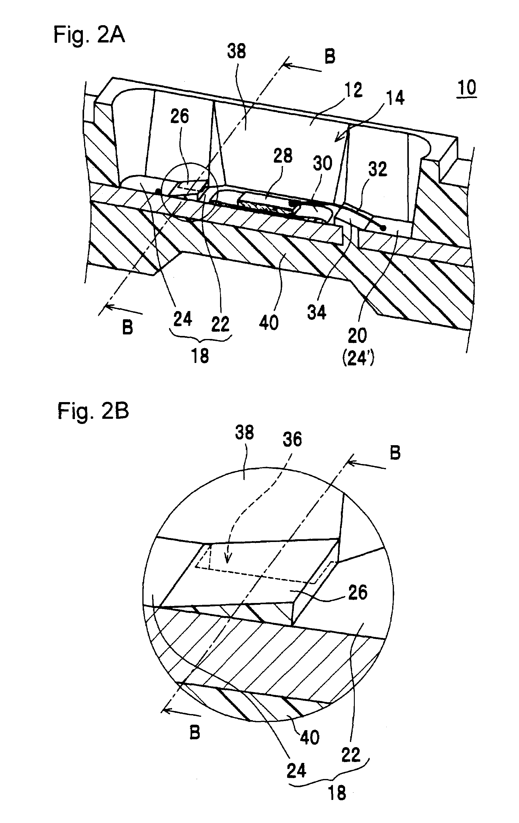
[0067]FIG. 1 and FIG. 2A show a mid stage of the process of manufacturing the semiconductor device according to the first embodiment, which becomes as shown in FIG. 6 in the final state. The semiconductor device 10 shown in FIG. 6 is extremely thin and is used as a thin light emitting device which uses a semiconductor light emitting element as the semiconductor element 28.

[0068]The semiconductor device 10 of the first embodiment comprises a housing 12 having a recess 14, a first lead electrode 18 and a second lead electrode 20 which are exposed on the bottom surface 16 of the recess 14. The first lead electrode 18 has a die bonding area 22 and a wire bonding area 24, while these areas are divided by a first wall 26 formed on the surface of the first lead electrode 18 so as to traverse the first lead electrode 18. The second lead electrode 20 is constituted from a wire bonding area 24′ only without die bonding area. A second wall 34 is formed to protrude between the first lead electr...

second embodiment

[0102]The semiconductor device of the second embodiment has a V groove 50 formed on the surface of the first lead electrode 18 as shown in FIG. 7A and FIG. 7B. The V groove 50 is located just below the first wall 26. The semiconductor device 10 of the second embodiment is similar to the first embodiment except for the first lead electrode 18 and the first wall 26.

[0103]As shown in FIG. 7A through FIG. 7C, the first wall 26 extends across the surface of the first lead electrode 18 and is bonded on both ends thereof with the side wall 38 of the housing 12. In the second embodiment, the V groove 50 is formed on the surface of the first lead electrode 18, and the first wall 26 is formed on the V groove 50. The V groove 50 is preferably formed along the first wall 26 that separates the die bonding area 22 and the wire bonding area 24. In this case, the V groove 50, together with the first wall 26, separates the surface of the first lead electrode 18 into the die bonding area 22 and the w...

third embodiment

[0108]The first embodiment employs the notch 36 and the second embodiment employs the V groove 50. The semiconductor device of the third embodiment has both the notch 36 and the V groove 50 formed in the first lead electrode 18 as shown in FIG. 8A and FIG. 8B. With other respects, the third embodiment is similar to the first and second embodiments. Details of the notch 36 and the V groove 50 are also similar to those of the first and second embodiments except for the points described below.

[0109]As shown in FIG. 8A through FIG. 8C, the first wall 26 extends across the surface of the first lead electrode 18 and is bonded with the side wall 38 of the housing 12 on both ends.

[0110]In the third embodiment, the rectangular notch 36 is formed in an edge 181 of the first lead electrode 18 at a position where the first wall 26 is to be formed. This constitution, similarly to the notch 36 of the first embodiment, achieves the effect of improving the bonding between the first wall 26 and the ...


PUM


Abstract

The present invention provides a semiconductor device capable of preventing an adhesive for die bonding from flowing to wire bonding area.The semiconductor device of the present invention comprises a semiconductor element 28 having a pair of electrodes, a housing 12 having the recess 14 for accommodating the semiconductor element 28, a first lead electrode 18 and the second lead electrode 20 which are exposed on the bottom of the recess 14, an adhesive layer 30 for die bonding between the semiconductor element 28 and the first lead electrode 18, and electrically conductive wires 32 for wire bonding between one electrode of the pair of electrodes of the semiconductor element and the first lead electrode 18 and between the other electrode and the second lead electrode 20, wherein the housing 12 has the wall 26 formed to extend across the bottom surface of the recess 14 so as to divide the surface of the first lead electrode 18 into a die bonding area 22 and a wire bonding area 24, and the first lead electrode 18 has the notch 36 which is formed by cutting off a portion of an edge of the first lead electrode 18 and located at least just below the wall 26, while the wall 26 and the bottom portion 40 of the housing 12 are connected to each other through the notch 36.

Description

BACKGROUND OF THE INVENTION[0001]1. Field of the Invention[0002]The present invention relates to a semiconductor device having a semiconductor element mounted in a housing thereof, and particularly to a semiconductor light emitting device employing a semiconductor light emitting element and a semiconductor light receiving device used as photo sensor or the like.[0003]2. Description of the Related Art[0004]Semiconductor devices currently available include a semiconductor light emitting device which has a semiconductor light emitting element mounted in a housing. The housing has a recess for accommodating the semiconductor light emitting element, and exposed on the surface of the recess are a pair of lead electrodes which are connected to the electrodes of the semiconductor light emitting element. The semiconductor light emitting element is mounted in the housing by die bonding the substrate side of the semiconductor light emitting element onto one of the lead electrodes by means of a...

Claims


Application Information

Patent Timeline
Patent Type & Authority Patents(United States)
IPC IPC(8): H01L23/52H01L33/62H01L33/56
CPCB29C45/14639H01L23/49861H01L24/48H01L33/486H01L33/62H01L2924/07802H01L2224/45169H01L24/45H01L2224/73265H01L2224/48091H01L2224/32245H01L2224/45147H01L2224/45144H01L2224/45124H01L2924/01023H01L2924/01006H01L2924/01005H01L2924/01082H01L25/167H01L31/0203H01L2224/48097H01L2224/48247H01L2924/01013H01L2924/01029H01L2924/01033H01L2924/01047H01L2924/0105H01L2924/01078H01L2924/01079H01L2924/00014H01L2924/00H01L2924/12035H01L2924/12041H01L2224/85951H01L2924/19107H01L2224/48997H01L2924/181H01L2224/48465H01L2224/85399H01L2224/05599
Inventor YAMAMOTO, SAIKINII, IKUYAUKAWA, HIROAKI
Owner NICHIA CORP
Why Eureka
Try Eureka