
Eureka
For R&D, Eureka makes reading and utilizing patents & technical documents easy.
Eureka AIR
Designed for self-driven R&D workflows. Generate viable solutions, solve complex R&D challenges, empower your innovation with AI.

Eureka Materials
Designed for material experts only. Revolutionize your material R&D, from search, analyze, to developing new materials.

TechResearch
Generate reliable direction feasibility study reports for your R&D in just a few steps.

TechSeek
Discover and master advanced knowledge NOW. Basics, ideas, possibilities, all at once.

TechMind
As an expert in R&D Theories, TechMind can generates customized viable solutions instantly.

TechRisk
Analyze your overall solution with one click, know your potential R&D risks in advance.

TechMonitor
Get weekly tech updates, stay abreast of the latest tech innovations and key insights.
Component comprising a large number of light-emitting-diode chips
- Summary
- Abstract
- Description
- Claims
- Application Information
AI Technical Summary
Benefits of technology
Problems solved by technology
Method used
Image

Examples
Example
DETAILED DESCRIPTION OF THE DRAWINGS
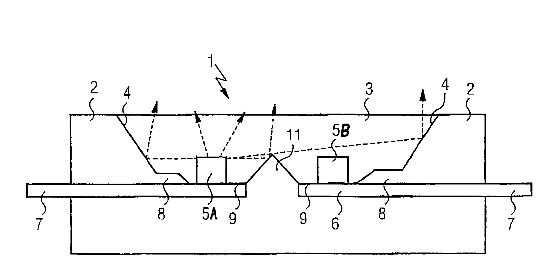
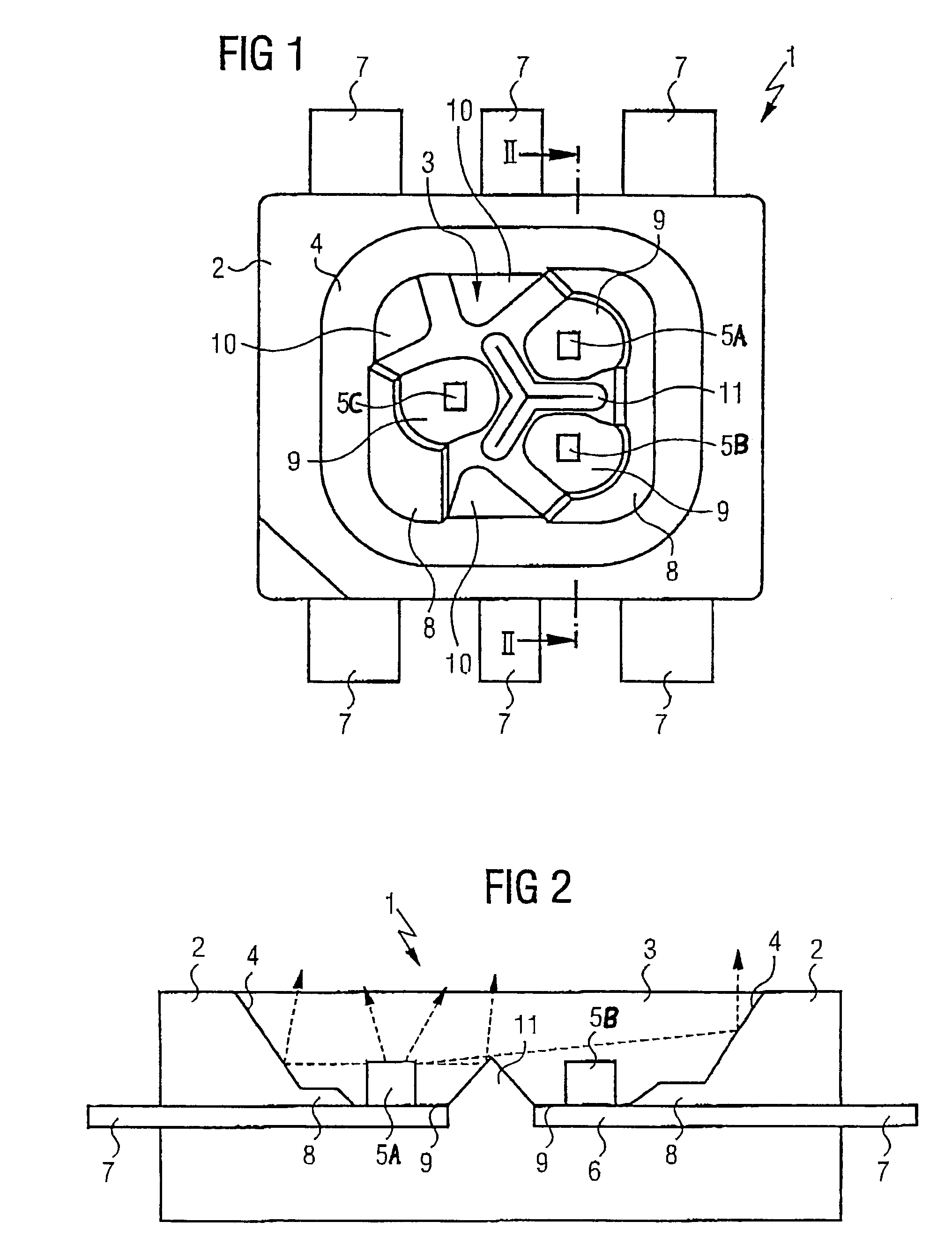
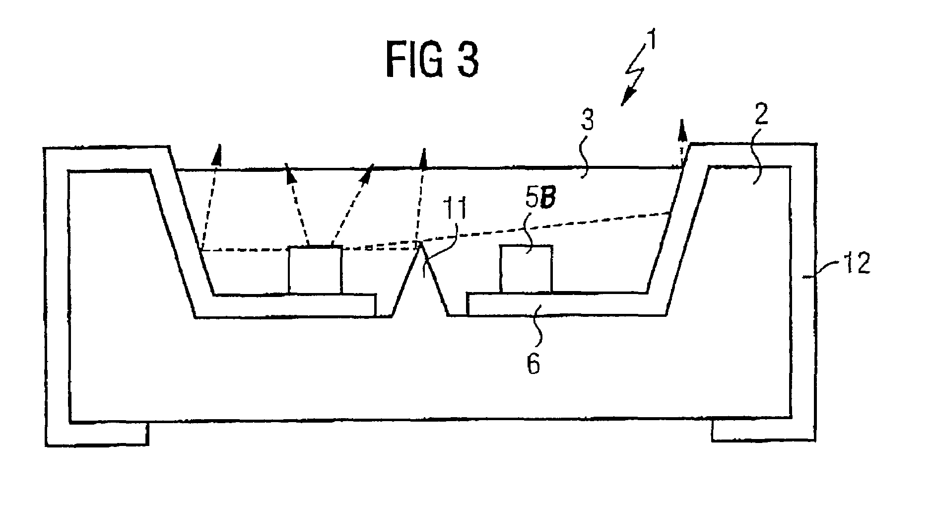
[0011]FIG. 1 shows a top view of a device 1, which is described in further detail below in conjunction with FIGS. 1 and 2. The device 1 has a housing 2 in which a cavity 3 is made. The cavity 3, with its sloped side walls 4, serves as a reflector for the light emitting diode chips 5A, 5B and 5C (referenced jointly as diode chips 5) which are arranged in the cavity 3. The light emitting diode chips 5 are arranged on a leadframe 6, whose connection elements 7 protrude laterally out of the housing 2. Some portions of the leadframe 6 are located beneath cover layers 8, which serve to fix the leadframe 6. The leadframe 6 is furthermore subdivided into individual mounting areas 9 for the light emitting diode chips 5 and bond pads 10 for the bond wires used for bonding the light emitting diode chips 5. The bond wires used for connecting the light emitting diode chips 5 are not shown in FIGS. 1 and 2.
[0012]In the arrangement shown in FIG. 1, there are sev...
PUM
 Abstract
Description
Claims
Application Information
 - R&D Engineer
- R&D Manager
- IP Professional
- Industry Leading Data Capabilities
- Powerful AI technology
- Patent DNA Extraction
Browse by: Latest US Patents, China's latest patents, Technical Efficacy Thesaurus, Application Domain, Technology Topic, Popular Technical Reports.
© 2024 PatSnap. All rights reserved.Legal|Privacy policy|Modern Slavery Act Transparency Statement|Sitemap|About US| Contact US: help@patsnap.com