Module assembly for multiple die back-illuminated diode

a back-illuminated diode and module technology, applied in the field of computed tomography, can solve the problems of placing physical limits on the number and size and increasing the density of traces and bond pads to an unattractive level

Inactive Publication Date: 2008-10-21
GENERAL ELECTRIC CO
View PDF14 Cites 14 Cited by
  • Summary
  • Abstract
  • Description
  • Claims
  • Application Information

AI Technical Summary

Problems solved by technology

As the number of elements in arrays increases, the density of the traces and bond pads increases to an unattractively high level near the edge of the photodiode array.
This places some physical limits on the number and size of traces and bond pads that can be made using top surface contacts.

Method used


Image

  • Module assembly for multiple die back-illuminated diode
  • Module assembly for multiple die back-illuminated diode
  • Module assembly for multiple die back-illuminated diode

Examples


Embodiment Construction

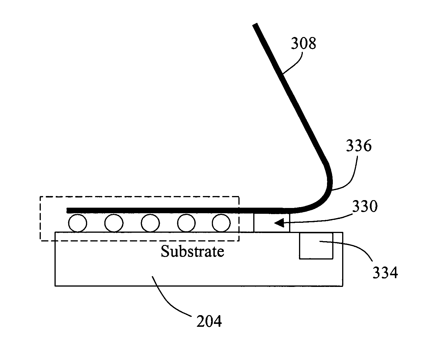
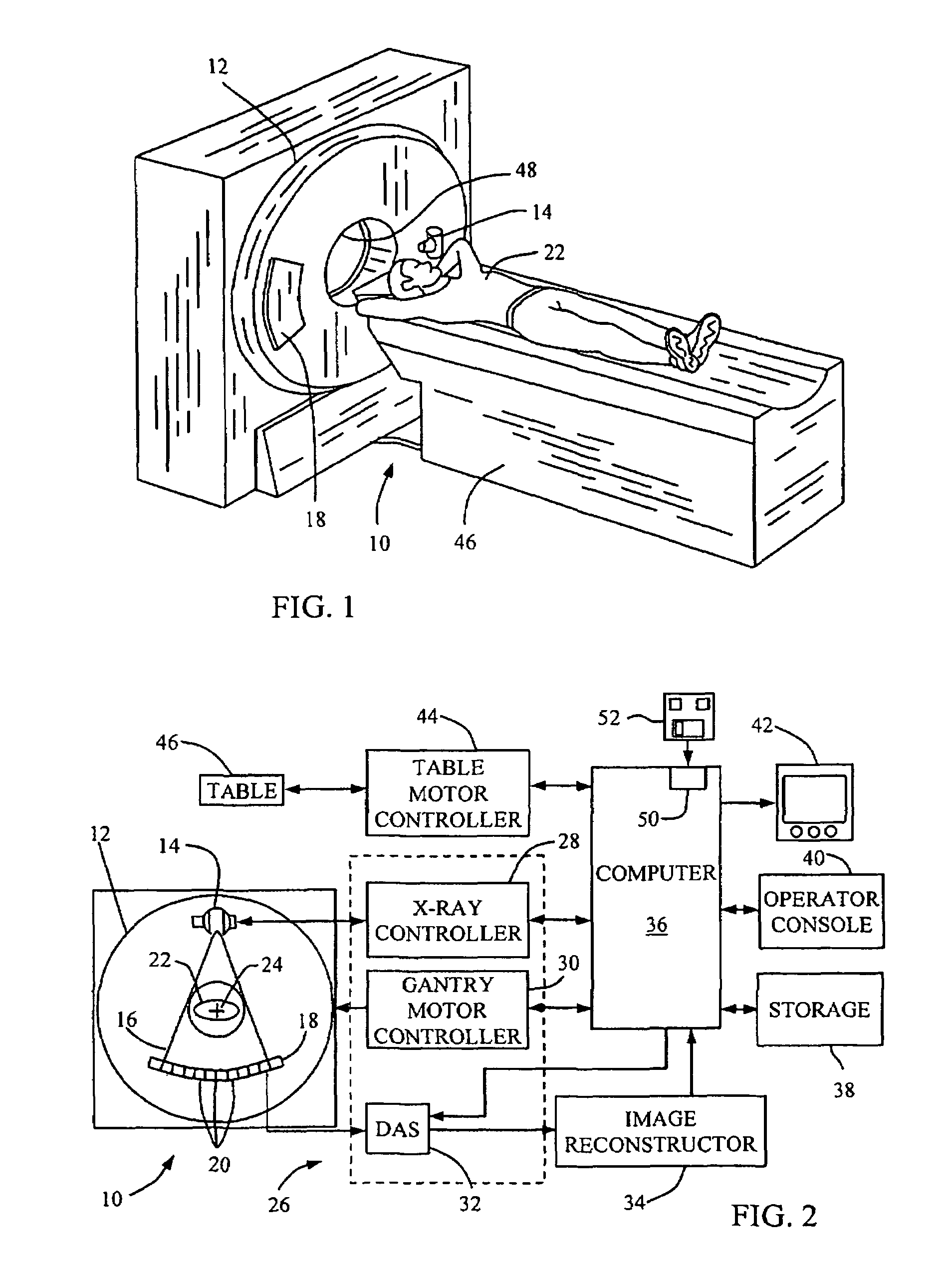
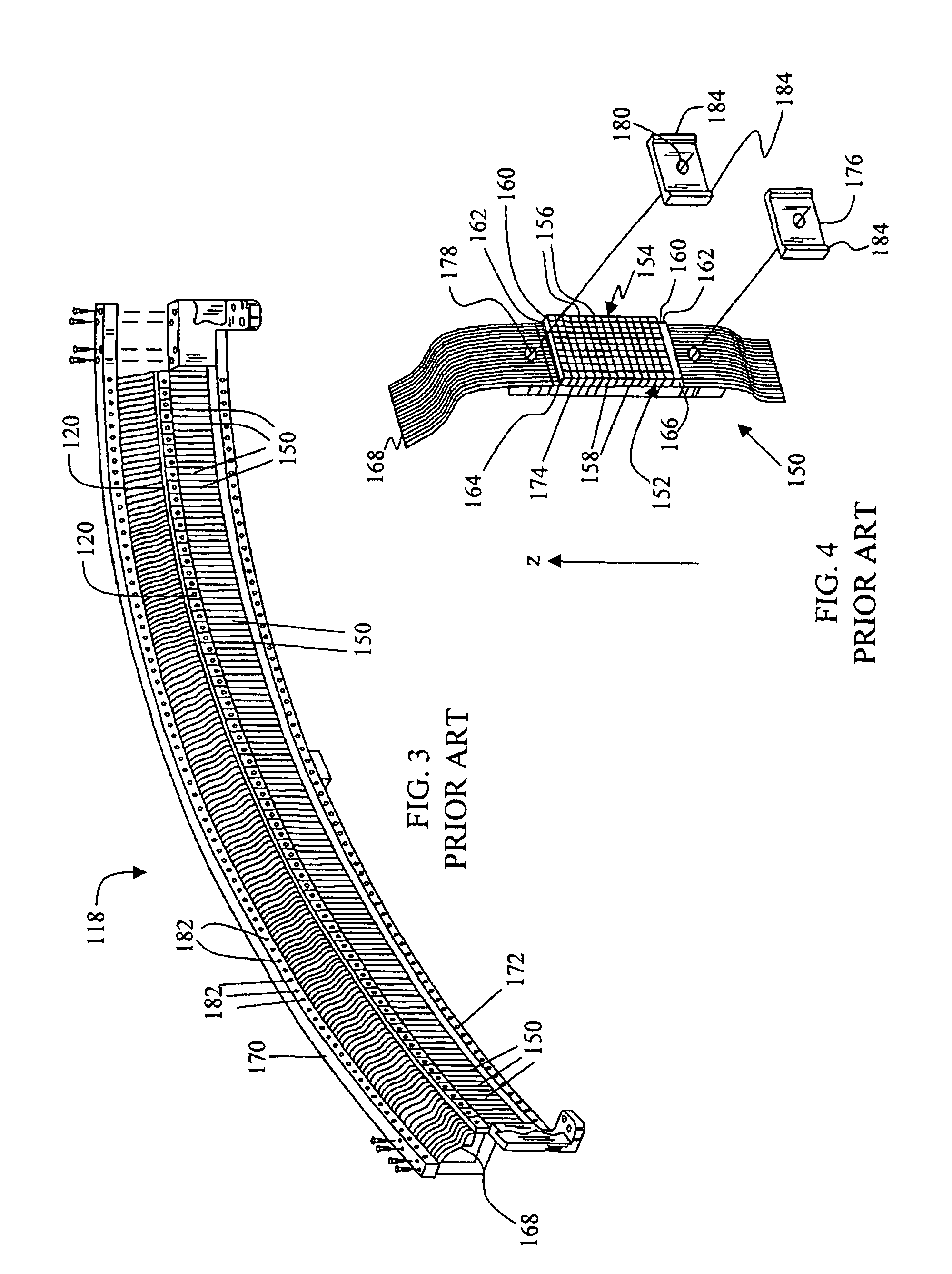
[0019]There are herein provided radiation detection methods and apparatus useful for imaging systems such as, for example, but not limited to a Computed Tomography (CT) System. The apparatus and methods are illustrated with reference to the figures wherein similar numbers indicate the same elements in all figures. Such figures are intended to be illustrative rather than limiting and are included herewith to facilitate explanation of an exemplary embodiment of the apparatus and methods of the invention.

[0020]In some known CT imaging system configurations, a radiation source projects a fan-shaped beam which is collimated to lie within an X-Y plane of a Cartesian coordinate system and generally referred to as an “imaging plane”. The radiation beam passes through an object being imaged, such as a patient. The beam, after being attenuated by the object, impinges upon an array of radiation detectors. The intensity of the attenuated radiation beam received at the detector array is dependen...


PUM


Abstract

A computerized tomography imaging scanner module includes a plurality of scintillators, a plurality of back-illuminated photodiodes optically coupled with the scintillators, a multi-layer substrate having a plurality of substrate electrical conductors to which the photodiodes are electrically coupled, wherein each of the plurality of substrate conductors is connected to a different one of the back-illuminated photodiodes, and a flexible cable having a plurality of flex electrical conductors to which the substrate is electrically coupled, wherein each of the plurality of flex electrical conductors is connected to a different output of the multi-layer substrate.

Description

BACKGROUND OF THE INVENTION[0001]This invention relates generally to medical imaging systems, and more particularly to computed tomography (CT). Although the application subject matter finds particular use in x-ray systems, the invention may also find use in connection with other imaging modalities.[0002]Modern CT scanners typically employ thousands of x-ray detectors to convert x-ray energy to electrical signals. A typical detector may include an array of scintillators attached to an array of semiconductor photodiodes which detect light or other ionizing radiation on their front surface. Some implementations have configurable detectors wherein signal currents from multiple individual photodiodes can be combined for further processing in a single amplifier channel. This arrangement permits the detection area for an individual pixel to be varied, using externally controlled electrical switches (field effect transistors, or FETs). The bond pads, for electrical connection to the FETs, ...

Claims


Application Information

Patent Timeline
Patent Type & Authority Patents(United States)
IPC IPC(8): H01L31/00
CPCG01T1/249H01L27/1464H01L27/14618H01L27/14634H01L27/1469G01T1/2018H01L21/563H01L24/81H01L24/83H01L27/14663H01L2224/13144H01L2224/73203H01L2224/8121H01L2224/81815H01L2224/83851H01L2924/01079H01L2924/01322H01L2224/2919H01L2924/00014H01L2924/12043H01L2224/73204H01L2924/14H01L2224/05573H01L2224/05568H01L2224/0554H01L2224/06131G01T1/20182H01L2924/00H01L2224/05599H01L2224/0555H01L2224/0556
Inventor ZEMAN, GREGORY SCOTTBABU, BAIJU ZACHARIANARAYANASWAMY, MAHESH RAMANHOFFMAN, DAVID MICHAELGRAVES, BRIAN JOSEPH
Owner GENERAL ELECTRIC CO
Why Eureka
Try Eureka