Forming ultra-shallow junctions

a junction and ultra-shallow technology, applied in the field of semiconductor devices, can solve the problems of lateral diffusion of dopants and other problems, and achieve the effect of reducing the number of junctions

Inactive Publication Date: 2008-11-25
INTEL CORP
View PDF14 Cites 67 Cited by
  • Summary
  • Abstract
  • Description
  • Claims
  • Application Information

AI Technical Summary

Problems solved by technology

However, the lateral diffusion of the dopants may also be restricted by the above annealing process.
This may be undesirable in the case where overlap of a gate electrode over tip extensions is insufficient for optimal performance of, e.g. a MOS-FET.

Method used


Image

  • Forming ultra-shallow junctions
  • Forming ultra-shallow junctions
  • Forming ultra-shallow junctions

Examples


Embodiment Construction

[0011]A process for fabricating semiconductor devices and the resultant devices are described. In the following description, numerous specific details are set forth, such as specific dimensions and chemical regimes, in order to provide a thorough understanding of the present invention. It will be apparent to one skilled in the art that the present invention may be practiced without these specific details. In other instances, well-known processing steps, such as patterning steps or wet chemical cleans, are not described in detail in order to not unnecessarily obscure the present invention. Furthermore, it is understood that the various embodiments shown in the figures are illustrative representations and are not necessarily drawn to scale.

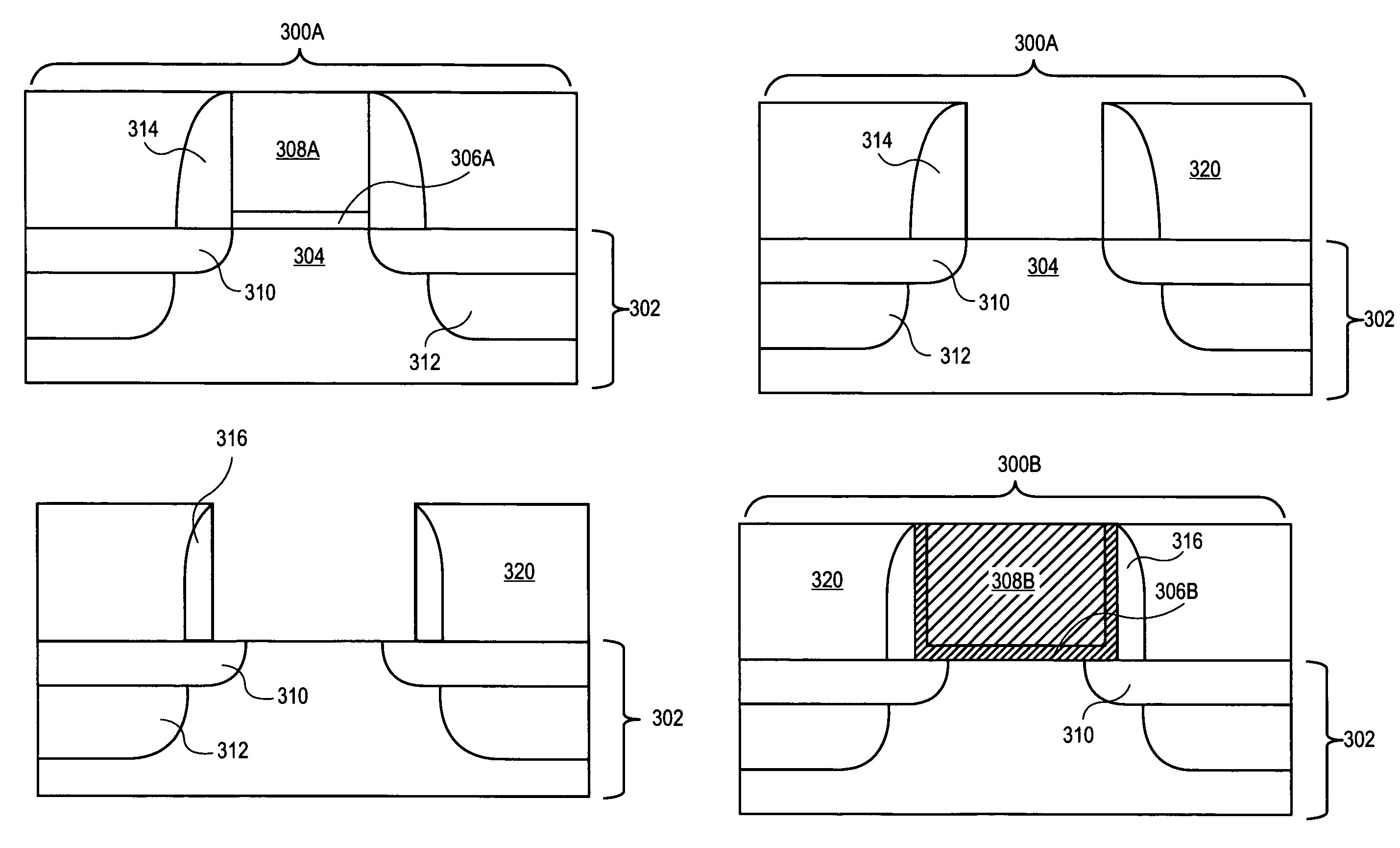
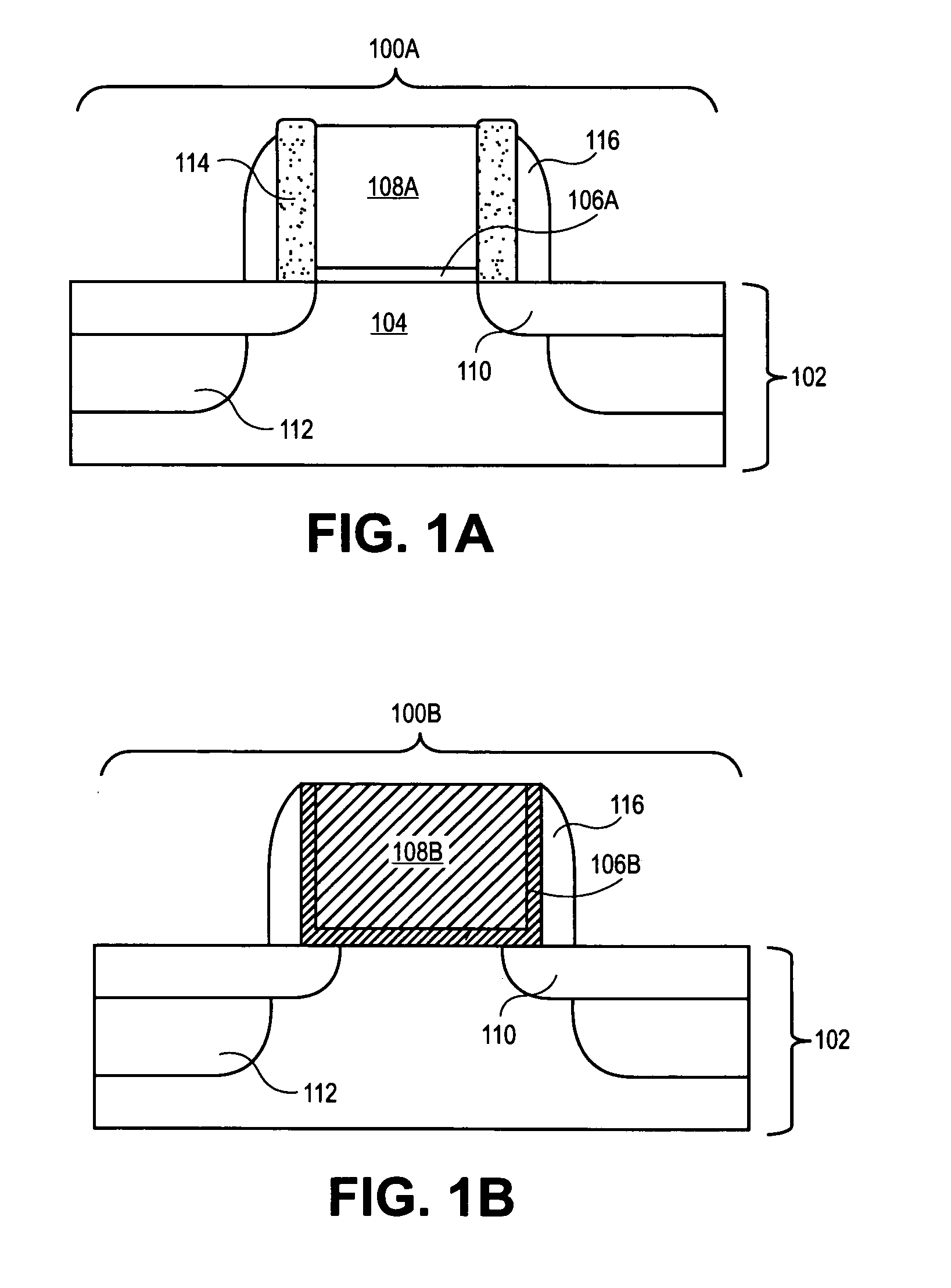
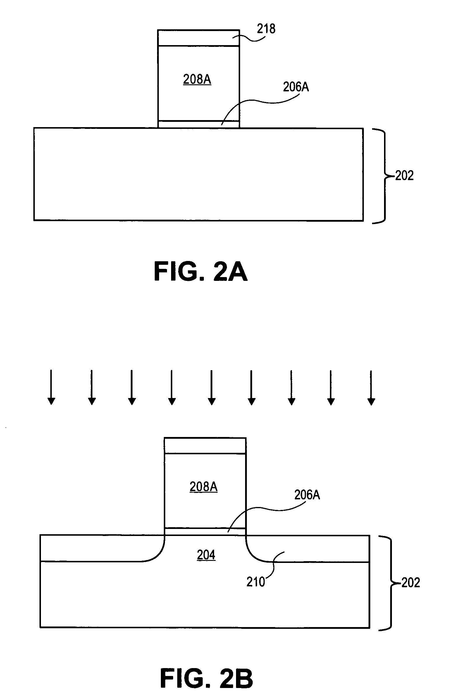
[0012]Disclosed herein is a method to form ultra-shallow junctions for semiconductor devices. Laser annealing of dopant impurity atoms implanted into a substrate may activate the dopant impurity atoms, i.e. cause them to be substitutionally integrat...


PUM


Abstract

A method to form an ultra-shallow junction is described. In one embodiment, a replacement gate process is utilized to enable the overlap of a gate electrode over the regions of a semiconductor substrate where tip extensions reside. In another embodiment, a sacrificial spacer is utilized in conjunction with the replacement gate process. In one embodiment, an initial gate electrode is formed with a gate length smaller than the desired final gate length and is subsequently replaced with an expanded gate electrode having the desired gate length.

Description

BACKGROUND OF THE INVENTION[0001]1) Field of the Invention[0002]The invention is in the field of Semiconductor Devices.[0003]2) Description of Related Art[0004]For the past several years, the performance of semiconductor devices, such as Metal Oxide Semiconductor Field-Effect Transistors (MOS-FETs), has been greatly enhanced by the incorporation of shallow junctions into the active portions of a semiconductor substrate, e.g. the use of shallow tip extensions. The presence of such shallow junctions may greatly enhance the rate at which charge migrates in a channel when a semiconductor is in an ON state.[0005]In the drive for ever-shallower junction depths, laser annealing of a dopant-implanted region of a semiconductor substrate may be utilized. Under appropriate annealing conditions, a laser anneal process may activate dopants, i.e. cause them to be substitutionally incorporated into the lattice of a substrate material, with negligible diffusion of the dopants into other regions of ...

Claims


Application Information

Patent Timeline
Patent Type & Authority Patents(United States)
IPC IPC(8): H01L21/336H01L21/4763
CPCH01L29/42392H01L29/6653H01L29/66545H01L29/66553H01L29/66795H01L29/7836H01L29/785H01L29/7851
Inventor KAVALIEROS, JACK T.LIU, MARK Y.DATTA, SUMAN
Owner INTEL CORP
Why Eureka
Try Eureka