Method and apparatus for preventing image artifacts

a technology of image artifacts and detection methods, applied in the direction of color television details, television system details, television systems, etc., can solve the problems of reducing the efficiency affecting the accuracy so as to prevent image artifacts during image readout and prevent saturation of pixel sensing electronics

Inactive Publication Date: 2009-07-14
GENERAL ELECTRIC CO
View PDF7 Cites 2 Cited by
  • Summary
  • Abstract
  • Description
  • Claims
  • Application Information

AI Technical Summary

Benefits of technology

[0012]A preferred embodiment of the present invention provides a method for preventing image artifacts during image readout from a solid state image sensor. The method includes the steps of determining an end-of-frame time indicative of image readout completion, determining a beginning-of-frame time indicative of image readout initiation, and resetting a charge accumulator of the pixel sensing electronics at least once between the end-of-frame time and the beginning-of-frame time to prevent saturation of the pixel sensing electronics.
[0013]A further preferred embodiment of the present invention provides a pixel sensing subsystem for a solid state image sensor. The pixel sensing subsystem includes frame timing logic that produces a frame timing signal indicative of an end-of-frame time and a beginning-of-frame time and reset logic that produces a reset signal for a charge accumulator of the pixel sensing electronics. The reset logic asserts the reset signal at least once between the end-of-frame time and the beginning-of-frame time to prevent saturation of the pixel sensing electronics.
[0014]Another preferred embodiment of the present invention provides a solid state image sensor. The image sensor includes an array of pixels organized into rows and columns, a row enable line for each row of pixels, and a column sense line for each column of pixels. The image sensor further includes pixel sensing electronics coupled to each column sense line, row enable logic producing a row enable signal on the row enable lines and asserted during readout of a row of pixels coupled to a particular row enable line, and frame timing logic that produces a frame timing signal indicative of an end-of-frame time and a beginning-of-frame time. The solid state image sensor also includes reset logic that produces a reset signal coupled to individual charge accumulators of the pixel sensing electronics. The reset signal is asserted at least once between the end-of-frame time and the beginning-of-frame time to prevent saturation of the pixel sensing elements.

Problems solved by technology

However, because the switch is made from amorphous silicon, a relatively large amount of charge remains in the channel (“the retained charge”) and bleeds out slowly over time.
However, the operational-amplifier is limited by its power supply voltages.
Thus, if the operational-amplifier saturates, and can no longer supply charge to the feed back capacitor, the data line potential will change, thereby changing the bias across the pixel.
An error signal results.
While the operational-amplifier is saturated, the operational-amplifier temporarily loses control over its input and the data line potential.
In other words, the operational-amplifier cannot immediately restore the desired potential to the data line.
As a result, many subsequent pixel readouts in a column are corrupted by the error signal, resulting in “white streaks” in the image read from the array.

Method used


Image

  • Method and apparatus for preventing image artifacts
  • Method and apparatus for preventing image artifacts
  • Method and apparatus for preventing image artifacts

Examples


Embodiment Construction

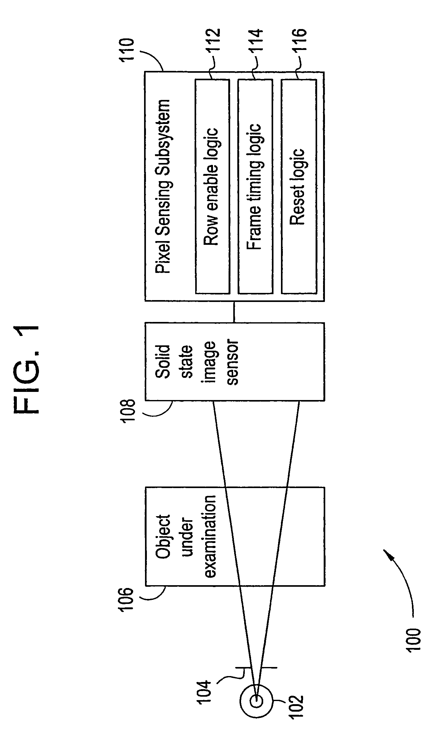
[0019]Turning now to FIG. 1, that figure illustrates a system level diagram of an X-ray imaging system 100. The imaging system 100 includes an X-ray source 102 and a collimator 104, which subject an object under examination 106 to X-ray photons. As examples, the X-ray source 102 may be an X-ray tube, and the object under examination 106 may be a human patient.

[0020]The X-ray imaging system 100 also includes a solid state image sensor 108 (“image sensor 108”) coupled to a pixel sensing subsystem 110. The pixel sensing subsystem 110 includes row enable logic 112, frame timing logic 114, and reset logic 116. The pixel sensing subsystem (and the associated row enable logic 112, frame timing logic 114, and reset logic 116) may be implemented in a single Application Specific Integrated Circuit (ASIC), gate array, Erasable Programmable Logic Device (EPLD), or the like.

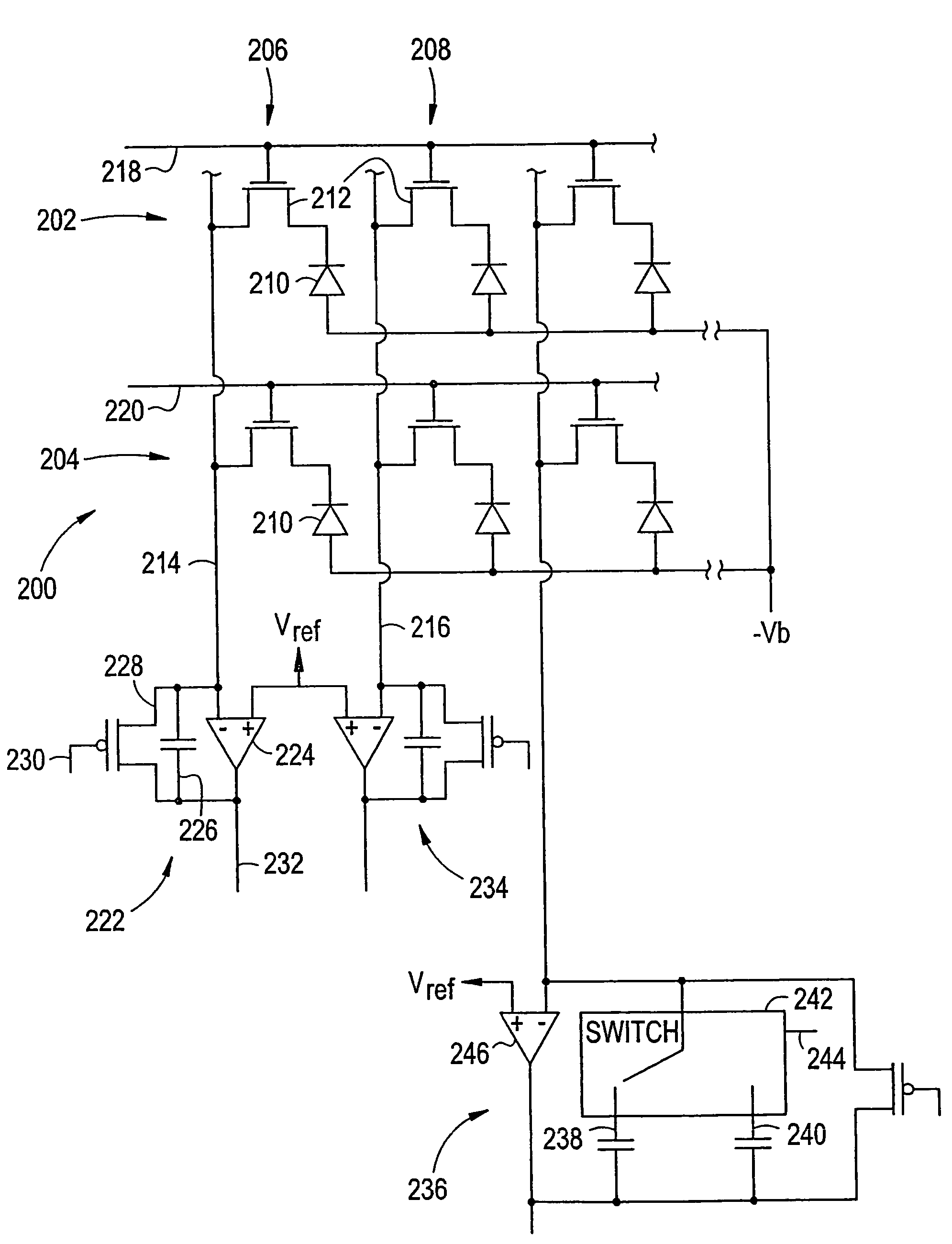
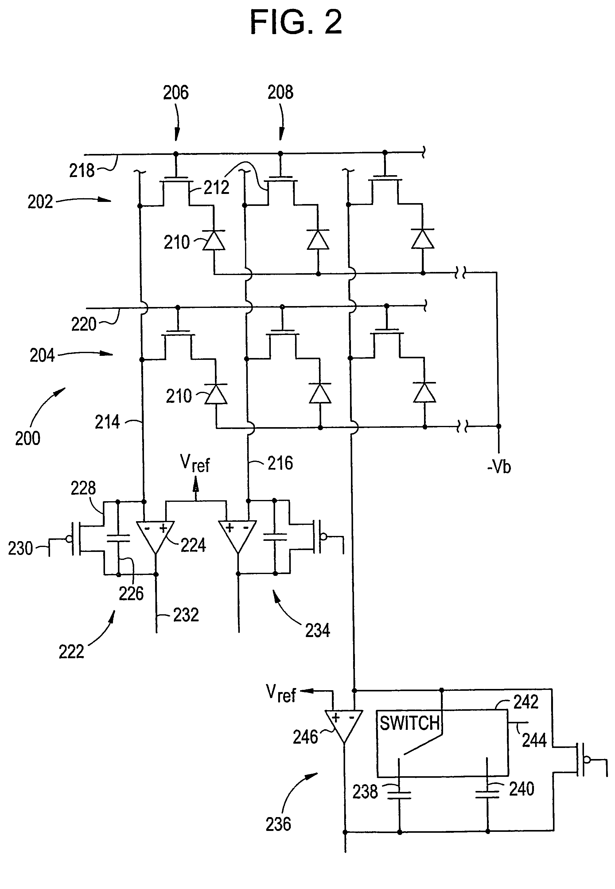
[0021]Turning next to FIG. 2, that figure depicts an array of pixels 200 of the image sensor 108. In particular, the array ...


PUM


Abstract

A pixel sensing subsystem for a solid state image sensor includes frame timing logic that produces a frame timing signal indicative of an end-of-frame time and a beginning-of-frame time and reset logic that produces a reset signal for a charge accumulator of pixel sensing electronics. The reset logic asserts the reset signal at least once between the end-of-frame time and the beginning-of-frame time to prevent saturation of the pixel sensing element.

Description

RELATED APPLICATIONS[0001]This application is a continuation of U.S. patent application Ser. No. 09 / 659,191, filed Sep. 11, 2000, now U.S. Pat. No. 6,888,969 entitled “Method and Apparatus for Preventing Image Artifacts”.FEDERALLY SPONSORED RESEARCH OR DEVELOPMENT[0002]Not Applicable.BACKGROUND OF THE INVENTION[0003]The present invention relates to solid state image sensors. In particular, the present invention relates to prevention of image artifacts in solid state X-ray detectors such as those used in medical diagnostic equipment.[0004]Present day solid state X-ray detectors are composed of an array of rows and columns of individual sensing elements (“pixels”) typically formed from amorphous silicon diodes. Each pixel is connected to a sense line (shared by a column of pixels) through a switch typically implemented as a thin film transistor or diode. Each row of pixels (a scan line) shares a separate control line, which activates and deactivates the switches for all the pixels in ...

Claims


Application Information

Patent Timeline
Patent Type & Authority Patents(United States)
IPC IPC(8): H04N3/14H04N5/335H04N5/32H04N5/359
CPCH04N5/3597H04N5/32H04N25/626
Inventor PETRICK, SCOTT WILLIAMSAUNDERS, ROLAND FREDERICKPERRY, DOUGLAS I.
Owner GENERAL ELECTRIC CO
Why Eureka
Try Eureka