Check patentability & draft patents in minutes with Patsnap Eureka AI!

Bonding configurations for lead-frame-based and substrate-based semiconductor packages

a technology of leadframe and substrate, applied in semiconductor devices, semiconductor/solid-state device details, electrical apparatus, etc., can solve the problems of increasing the net die count of the device during fabrication, increasing the cost of the chip, and increasing the likelihood of shorting between bonding wires

Active Publication Date: 2009-07-28
SAMSUNG ELECTRONICS CO LTD
View PDF14 Cites 0 Cited by
  • Summary
  • Abstract
  • Description
  • Claims
  • Application Information

AI Technical Summary

Benefits of technology

This configuration prevents wire-to-wire shorting, maintains acceptable bonding angles, and allows for a higher net die count per wafer, reducing manufacturing costs and increasing fabrication throughput without enlarging the chip.

Problems solved by technology

Therefore, the number of bonding pads placed at the edges of the chip die likewise increases, which places constraints on the chip packaging.
With the reduced distance S1 between wires in the corner regions, there is an increased likelihood of shorting between bonding wires in the corner regions during the final stages of chip packaging, a costly time at which to introduce defects in the fabrication process since manufacture of the chip is nearly completed at that time.
However, a bonding configuration in which the corner rule is applied results in an increased chip size if the bonding pad count is to be maintained.
This is contrary to design integration, and contrary to manufacturing throughput in which an optimal “net die” count, or number of chips per wafer, is desired.
Accordingly device fabrication costs are proportionally increased.

Method used


Image

  • Bonding configurations for lead-frame-based and substrate-based semiconductor packages
  • Bonding configurations for lead-frame-based and substrate-based semiconductor packages
  • Bonding configurations for lead-frame-based and substrate-based semiconductor packages

Examples


Embodiment Construction

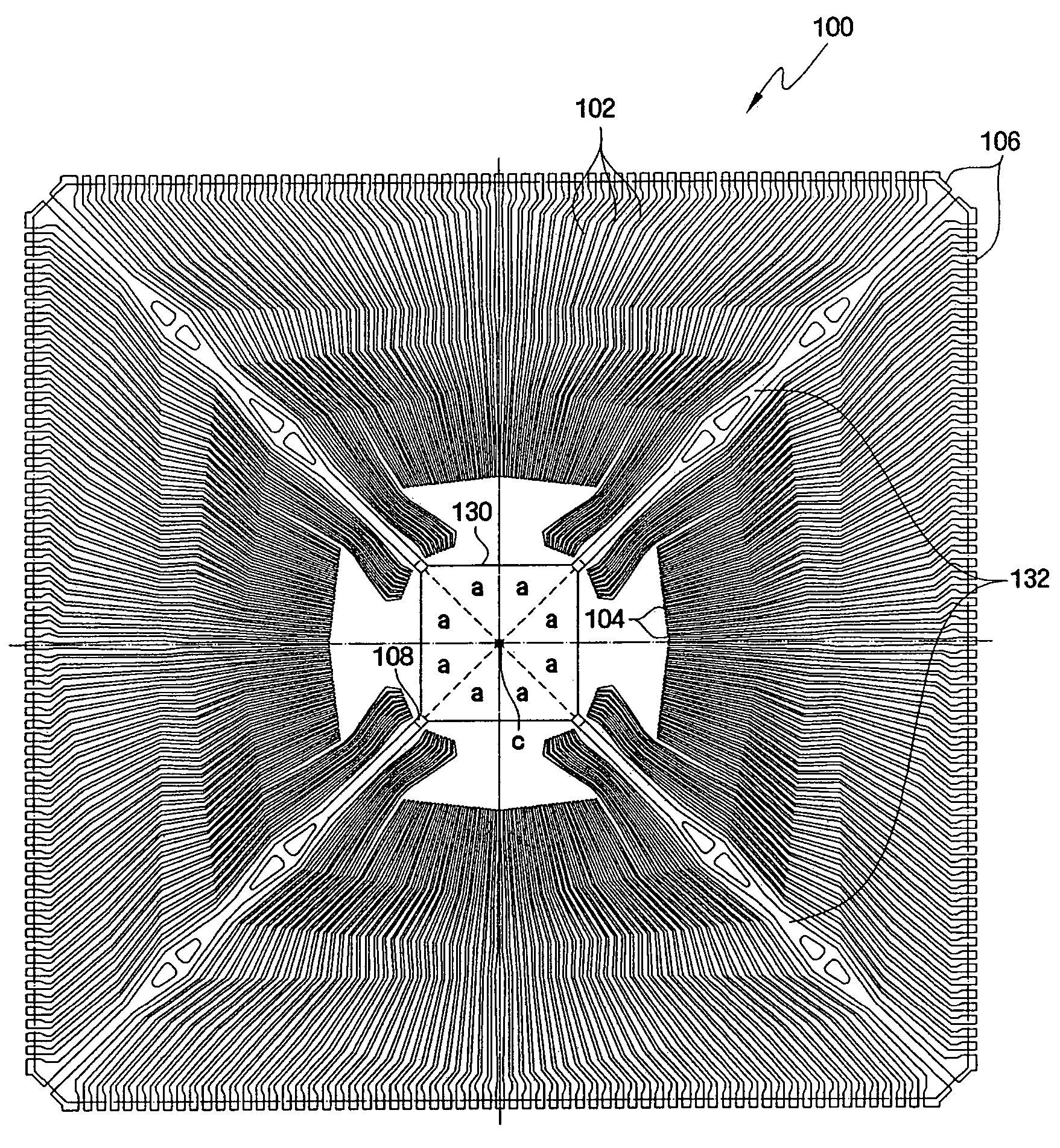
[0107]FIG. 3 is a plan view of a connecting board, or “lead frame”100, that is configured in accordance with the present invention. The lead frame 100 of the present invention includes a plurality of leads 102, each extending from a inner end 104 at an inner region of the lead frame to an outer end 106 at an outer region of the lead frame. The leads 102 of the lead frame 100 comprise a conductive metal or alloy, such as copper, aluminum, or gold, or other conductive materials or alloys. Inner ends 104 of the leads of the lead frame 100 surround a region 130 where a die pad or chip pad is to be mounted on the lead frame 100.

[0108]A plurality of tie bars 132 extend from four corners of the lead frame. Inner ends 108 of the tie bars 132 extend into the die pad region 130, for supporting a die pad or plate on which the die is mounted. The die pad region 130 has a center point c. Four quadrants surround the center point c, each quadrant comprising two octants a.

[0109]The example shown in...


PUM


Abstract

In a bonding configuration for a semiconductor device package, the bonding angles of the bonding wires are maintained within acceptable limits, without causing an increase in the chip die size, and without necessitating the use of the corner rule. In this manner, the occurrence of shorting between adjacent bonding wires can be mitigated or eliminated, and device net die count during fabrication can be increased.

Description

RELATED APPLICATIONS[0001]The application claims priority to Korean patent application 2004-58070, filed Jul. 24, 2004, the contents of which are incorporated herein by reference.BACKGROUND OF THE INVENTION[0002]The number of transistors that can be formed on an integrated circuit chip continues to increase with the trend toward higher integration. Accordingly, integrated circuits become more sophisticated and demand an increased number of input and output I / O terminals or leads. Therefore, the number of bonding pads placed at the edges of the chip die likewise increases, which places constraints on the chip packaging.[0003]In an integrated circuit die, the bonding pads are commonly placed at the perimeter of the chip. The die is mounted to a lead frame or package substrate, which in turn contains a number of pins or leads for distributing the signals from the bonding pads of the die to a circuit panel to which the chip package is mounted. The lead frame or package substrate include...

Claims


Application Information

Patent Timeline
Patent Type & Authority Patents(United States)
IPC IPC(8): H01L23/495
CPCH01L23/3107H01L23/3128H01L23/4951H01L23/49541H01L23/49838H01L24/06H01L24/32H01L24/49H01L24/85H01L23/49816H01L24/45H01L2224/05624H01L2224/05644H01L2224/05647H01L2224/32014H01L2224/32188H01L2224/32225H01L2224/32245H01L2224/45144H01L2224/45147H01L2224/48091H01L2224/48227H01L2224/48237H01L2224/48247H01L2224/48257H01L2224/4912H01L2224/49171H01L2224/73265H01L2224/85205H01L2224/92247H01L2924/01005H01L2924/01013H01L2924/01014H01L2924/01015H01L2924/01029H01L2924/01033H01L2924/01075H01L2924/01078H01L2924/01079H01L2924/01082H01L2924/014H01L2924/14H01L2924/15153H01L2924/15165H01L2924/1517H01L2924/15311H01L2924/1532H01L2924/19043H01L24/48H01L2924/00014H01L2924/01006H01L2224/48233H01L2224/48253H01L2924/0132H01L2924/0133H01L2924/15724H01L2924/15738H01L2924/15747H01L2224/29111H01L2224/48624H01L2224/48644H01L2224/48647H01L2224/48844H01L2224/48847H01L2224/2919H01L2924/15321H01L2224/05554H01L2224/78H01L2924/00H01L2924/01047H01L2924/0105H01L2224/48824H01L2924/00012H01L2924/15787H01L2924/181H01L24/73H01L2224/06179H01L23/495
Inventor JANG, KYUNG LAELEE, HEE SEOKKWON, HEUNG KYU
Owner SAMSUNG ELECTRONICS CO LTD
Features
  • R&D
  • Intellectual Property
  • Life Sciences
  • Materials
  • Tech Scout
  • Unparalleled Data Quality
  • Higher Quality Content
  • 60% Fewer Hallucinations
Learn More