Semiconductor integrated circuit layout structure

a technology of integrated circuits and layout structures, which is applied in the direction of semiconductor devices, semiconductor/solid-state device details, electrical apparatus, etc., can solve the problems of enormously affecting the layout structure of the ics, the process complexity and process cost are unavoidably increased, so as to simplify the layout design and simplify the layout design. , the effect of improving the layout structure of the semiconductor inv

Active Publication Date: 2016-11-10
UNITED MICROELECTRONICS CORP
View PDF3 Cites 21 Cited by
  • Summary
  • Abstract
  • Description
  • Claims
  • Application Information

AI Technical Summary

Benefits of technology

[0012]According to the present invention, a semiconductor INV layout structure, a semiconductor ND2 layout structure and a semiconductor XOR2 layout structure are respectively provided. In the semiconductor INV layout structure, the slot-type conductive structures and the island-type conductive structure are formed in one same layer. The slot-type conductive structures construct electrical connections between the sources / drains and other devices while the island-type conductive structure constructs electrical connection between the gate structure and other devices. By providing the slot-type conductive structures and the island-type conductive structure in one single layer, the present invention provides a semiconductor INV layout structure including a simplified layout design without affecting the required electrical connections, and thus fabrication for the semiconductor INV layout structure is improved. In the semiconductor ND2 layout structure provided by the present invention, the first wire structures extending along one direction and the second wire structures extending along at least two directions are formed in one same layer. By providing the first wire structures and the second wire structure in one single layer, the present invention provides a semiconductor ND2 layout structure including a simplified layout design without affecting the required electrical connections, and thus fabrication for the semiconductor ND2 layout structure is improved. In the semiconductor XOR2 layout structure provided by the present invention, the first conductive structures and the second conductive structures are formed in one same layer. An extending direction of the first conductive structures is parallel with an extending direction of the gate structures. The second conductive structures further include the island-type conductive structures and the slot-type conductive structures perpendicular to the gate structures. By providing the conductive structures including two extending directions perpendicular to each other and the island-type conductive structures formed in one single layer, the present invention provides a semiconductor XOR2 layout structure including a simplified layout design without affecting the required electrical connections, and thus fabrication for the semiconductor XOR2 layout structure is improved.

Problems solved by technology

It is found that the multiple patterning technology gives rise to process control challenges.
Thus, process complexity and process cost are unavoidably increased with the involvement of the multiple patterning technology.
Since those standard cells are essential elements for the ICs, layout structures of those standard cells enormously affect the whole layout structure of the ICs.

Method used


Image

  • Semiconductor integrated circuit layout structure
  • Semiconductor integrated circuit layout structure
  • Semiconductor integrated circuit layout structure

Examples


Embodiment Construction

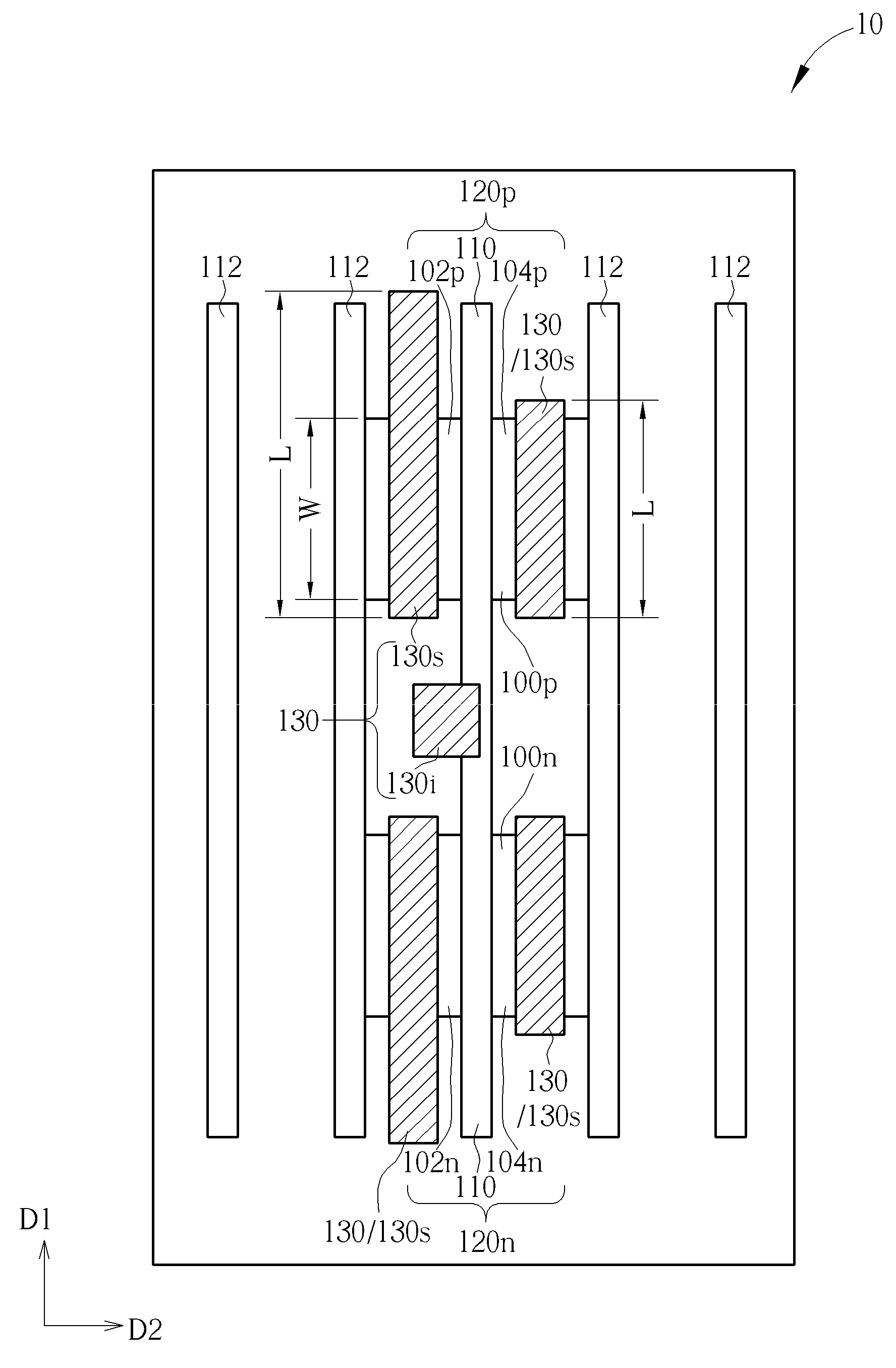
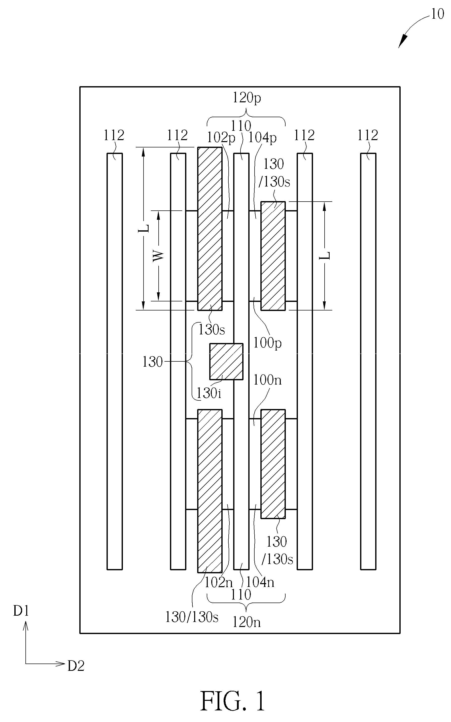
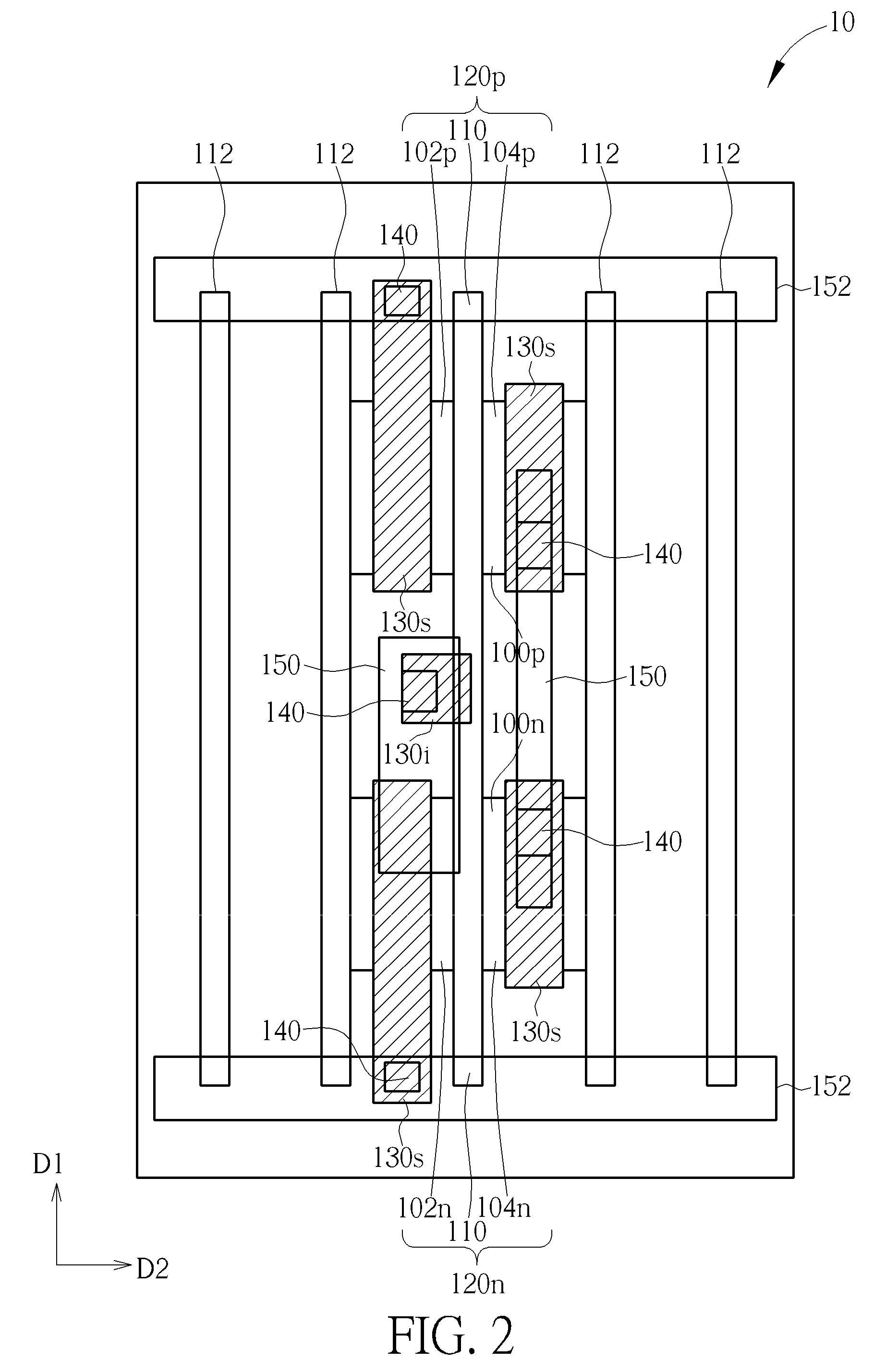
[0023]It will be understood that, although the terms, first, second, third, etc. may be used herein to describe various elements, components, regions, layers and / or sections, these elements, components, regions, layers and / or sections should not be limited by these terms. These terms are only used to distinguish one element, component, region, layer or section from another element, component, region, layer or section. Thus, a first element, component, region, layer or section discussed below could termed a second element, component, region, layer or section without departing from the teachings of the present invention. And it is noted that the drawings are provided for illustrative purposes, and as such, they are not to drawn to scale.

[0024]Please refer to FIGS. 1-3, FIG. 1 is a schematic drawing of a portion of a semiconductor INV layout structure provided by a preferred embodiment of the present invention, FIG. 2 is a schematic drawing of the semiconductor INV layout structure pro...


PUM


Abstract

A semiconductor integrated circuit layout structure includes a first active region, a second active region isolating from the first active region, a gate structure straddling the first active region and the second active region, and a plurality of conductive structures. The first active region at two opposite sides of the gate structure respectively forms a first source region and a first drain region. The second active region at two opposite sides of the gate structure respectively forms a second source region and a second drain region. The conductive structures include a plurality of slot-type conductive structures and one island-type conductive structure. The slot-type conductive structures are respectively formed on the first source region, the first drain region, the second source region and the second drain region. The island-type conductive structure is formed on the gate structure.

Description

CROSS REFERENCE TO RELATED APPLICATIONS[0001]This patent application claims the benefit under 35 U.S.C. §119(e) of U.S. Provisional Patent Application Ser. No. 62 / 158,534, which was filed on May 7, 2015. U.S. Provisional Patent Application Ser. No. 62 / 158,534 is incorporated herein by reference in its entirety.BACKGROUND OF THE INVENTION[0002]1. Field of the Invention[0003]The present invention relates to semiconductor integrated circuit (hereinafter abbreviated as IC) structures, and more particularly, to semiconductor IC structures of inverter (hereinafter abbreviated as INV), 2-input not-and gate (2-input NAND, hereinafter abbreviated as ND2) and 2-input exclusive-or gate (hereinafter abbreviated as XOR2).[0004]2. Description of the Prior Art[0005]Fabrication of microstructures requires tiny elements of precisely controlled size formed in a material layer of an appropriate substrate such as semiconductor substrate / layers, dielectric layers and / or metal layers. These tiny elements...

Claims


Application Information

Patent Timeline
Patent Type & Authority Applications(United States)
IPC IPC(8): H01L23/528H01L27/088H01L27/115H01L23/522H01L23/00H01L29/78H01L29/06
CPCH01L23/528H01L29/785H01L27/0886H01L29/0653H01L2224/48132H01L24/49H01L27/11521H01L2924/37001H01L23/5226H01L27/0207H01L27/11807H01L24/48H01L27/092H01L21/823871H01L27/0924H01L2924/00014H01L21/28518H01L29/0649H01L29/4983H01L2224/45015H01L2924/207H01L2224/45099
Inventor LIN, SHIH-CHINHUNG, KUEI-CHUNHU, JERRY CHE JENCHEN, MING-JUIHSU, CHEN-HSIEN
Owner UNITED MICROELECTRONICS CORP
Why Eureka
Try Eureka