Semiconductor device, manufacturing method of semiconductor device and module for optical device

A manufacturing method and semiconductor technology, which can be used in semiconductor devices, semiconductor/solid-state device components, semiconductor lasers, etc., and can solve problems such as scarring

Inactive Publication Date: 2005-12-14
SHARP KK
View PDF1 Cites 8 Cited by
  • Summary
  • Abstract
  • Description
  • Claims
  • Application Information

AI Technical Summary

Problems solved by technology

[0010] In a semiconductor device in Published Japanese Patent Application No. 2002-124589, there is a simple linear outlet section, however, problems may arise
[0011] The problem is that since the outlet path 70 provided in the semiconductor device in Published Japanese Patent Application No. 2002-124589 has a simple linear form, that is, extends in a linear manner, moisture can enter through the outlet path 70 during the cleaning step. device, foreign matter can enter the device together with water, and foreign matter can adhere to the surface of the main plane of the semiconductor chip 56 like dust, so it is possible to produce scars on the surface of the main plane of the semiconductor chip 56

Method used


Image

  • Semiconductor device, manufacturing method of semiconductor device and module for optical device
  • Semiconductor device, manufacturing method of semiconductor device and module for optical device
  • Semiconductor device, manufacturing method of semiconductor device and module for optical device

Examples


Embodiment 1

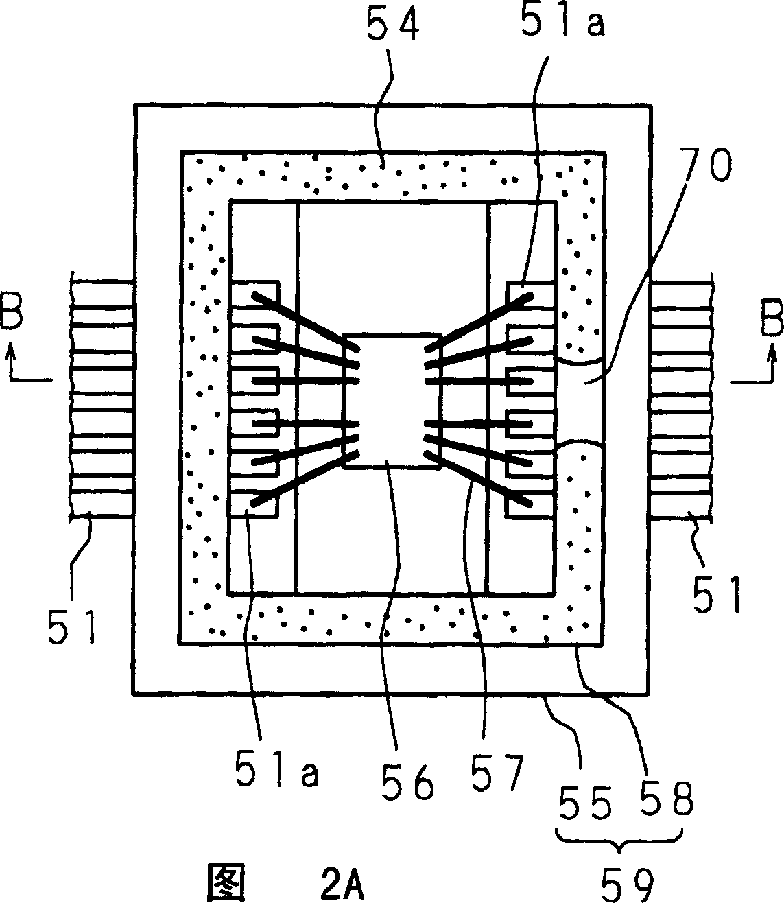
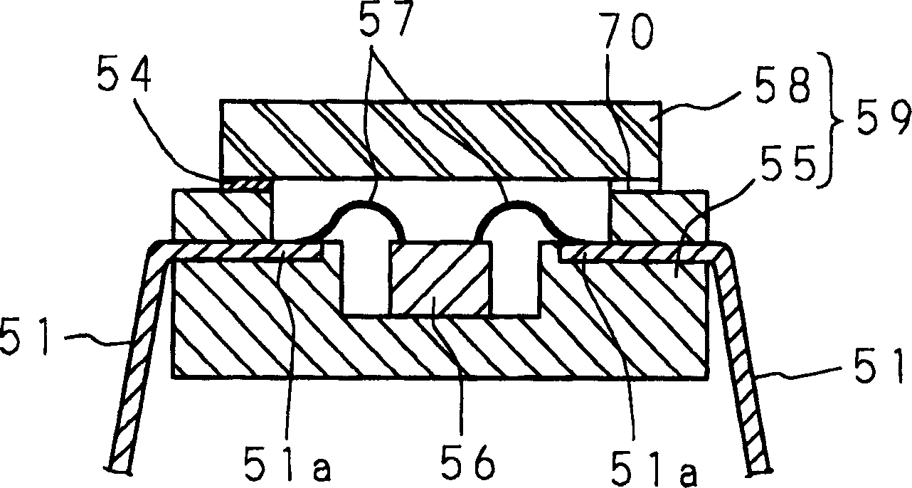
[0107] Figure 3A and 3B is a schematic diagram showing the structure of the solid-state imaging device according to Embodiment 1 of the present invention, in particular, Figure 3A A plan view showing the main plane (one plane) of the solid-state imaging device shown above, Figure 3B yes Figure 3A Sectional view along line B-B in . It should be noted that the joint part 5 is equipped with an outlet path 7 with a sealing function, which is a feature of the present invention and is marked with oblique lines in the following top view for ease of understanding.

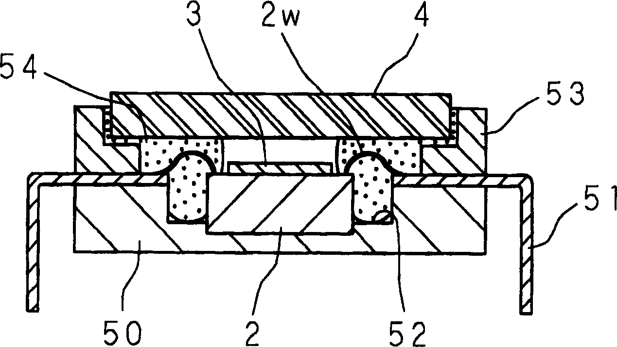
[0108] Figure 3A and 3B Among them, 1 indicates a solid-state imaging device, and the solid-state imaging device 1 includes the following main components: a solid-state imaging element 2 equipped with a semiconductor substrate (for example, a single crystal silicon substrate), which has a rectangular shape in plan, and is equipped with a semiconductor circuit; a cover portion 4 made of a transparent material (for ex...

Embodiment 2

[0128] Figure 8A to 8E, FIGS. 9A and 9B, and FIGS. 10A and 10B are schematic diagrams showing a method of manufacturing a solid-state imaging device according to Embodiment 2 of the present invention, in particular, Figure 8A 8E to 8E are schematic diagrams showing the forming steps of the cover portion, FIGS. 9A and 9B are schematic diagrams showing the state of the solid-state imaging element formed on the semiconductor wafer, and FIGS. 10A and 10B are diagrams showing Figure 8A A schematic diagram of a state in which the covering portion formed in FIG. 8E is combined with the main plane (surface having an effective pixel area) of the solid-state imaging element in FIGS. 9A and 9B .

[0129] Figure 8A A transparent sheet 40 is shown having a large area, made of eg a glass sheet. The large-area sheet 40 includes a plurality of covering portions corresponding to the region 40b (with the dividing line 40a as a boundary). When splitting in subsequent steps, the area corre...

Embodiment 3

[0144] Figure 11A and 11B , FIGS. 12A to 12C are schematic diagrams showing a method of manufacturing a solid-state imaging device according to Embodiment 3 of the present invention, in particular, Figure 11A and 11B 12A to 12C are schematic diagrams showing the steps of forming the covering part, and Figs. 12A to 12C are diagrams showing bonding Figure 11A and 11B A schematic diagram of the step of forming a covering portion to one plane (surface having an effective pixel area) of a solid-state imaging element formed on a semiconductor wafer.

[0145] Figure 11A A large area transparent sheet 40 is shown, formed for example from a glass sheet. The large-area sheet 40 includes a plurality of covering portions corresponding to areas 40b having a separation line 40a as a boundary. When in the subsequent division step, the area corresponding to the covered portion of the area 40b is adjusted to be the same size as the covered portion 4 in plan.

[0146] Figure 11B A ...


PUM


Abstract

The bonding portion bonding the main plane of the solid-state imaging element with the transparent cover portion and forming a hollow portion therebetween is equipped with: a first opening end portion on the hollow portion side; a second opening end portion on the outside; and a trap portion. The first open end portion, the trap portion and the second open end portion define an exit path. The form of the outlet path is not to connect the first open end portion with the second open end portion in a linear manner, but to connect the open end portions in the joint portion by a trap portion larger than the open end portion.

Description

technical field [0001] The present invention relates to a semiconductor device having a sealing function and equipped with an outlet path in a cover covering a semiconductor element; a method of manufacturing the semiconductor device; and a module of an optical device using the semiconductor device. Background technique [0002] Conventional light-receiving semiconductor devices, such as CCD (Charge Coupled Device) image sensors and CMOS (Complementary Metal Oxide Semiconductor) image sensors that convert optical signals into electrical signals, have Semiconductor elements or the like to prevent moisture, pollutants, etc. from entering the semiconductor elements from the outside. [0003] FIG. 1 is a cross-sectional view showing a structural view of a solid-state imaging device as an example of a conventional light-receiving semiconductor device. The solid-state imaging device shown in FIG. 1 includes a hollow package, which has a hollow portion (space), located on a base 5...

Claims


Application Information

Patent Timeline
Patent Type & Authority Applications(China)
IPC IPC(8): H01L23/02H01L27/14H01L23/04H01L31/0203
CPCH01L27/14618H01L2224/48091H01L2224/48247H01L2224/45144H01L2924/16195H01L2924/16235H01L2924/00014H01L2924/00
Inventor 塚本弘昌藤田和弥安留高志
Owner SHARP KK
Why Eureka
Try Eureka