Reliable BEOL integration process with direct CMP of porous SiCOH dielectric

a technology of porous sicoh dielectric and integrated circuit, which is applied in the direction of electrical apparatus, semiconductor devices, semiconductor/solid-state device details, etc., can solve the problems of affecting the overall chip performance, hm erosion and polishing potential, and affecting the reliability of prior art structures, so as to improve the reliability of porous ulk dielectric, reduce the conductivity, and improve the effect of reliability

Inactive Publication Date: 2007-08-07
GLOBALFOUNDRIES INC
View PDF2 Cites 24 Cited by
  • Summary
  • Abstract
  • Description
  • Claims
  • Application Information

AI Technical Summary

Benefits of technology

[0016]The present invention relates to methods of improving the fabrication of BEOL interconnect structures of the single or dual damascene type, in which there is no problem of HM retention or of conductivity between the metal lines after fabrication.
[0017]The present invention also relates to methods of improving the fabrication of BEOL interconnect structures of the single or dual damascene type, in which a HM is not used, and in which the CMP-induced damage to ULK dielectrics is repaired to make dielectrics with high reliability.
[0018]The present invention further relates to the repair of the plasma damage caused by a PPFCC step to the ULK dielectric, again to improve the reliability of the structure. The present invention even further relates to methods for improving the fabrication of BEOL interconnect structures of the single or dual damascene type in which paths for increased conductivity between the metal lines are eliminated. The elimination of such high conductivity paths results in a highly reliable structure.

Problems solved by technology

However, fabrication and reliability problems are associated with these prior art structures.
Two specific problems with porous ultra low k (ULK) dielectric films and integration using a HM layer are capacitance and HM retention; porous ULK dielectrics may be made using a sacrificial porogen phase in which the as deposited film contains 100% of the sacrificial phase, while the cured ULK has essentially all of this phase removed, and contains only a few percent or less of the sacrificial phase.
This could lead to potential HM erosion and polishing into the ULK dielectric, thus directly exposing the ULK dielectric to the CMP slurry.
The aforesaid erosion and polishing could adversely impact the overall chip performance by increasing the interline leakage (conductivity) and the capacitance (due to a higher film dielectric constant).
Further, the topography (roughness) generated at a lower level could result in other CMP or lithography issues at the subsequent upper level(s) in an integrated multilevel build.
A third problem using porous ULK dielectrics is CMP damage to the HM layer, which may exist in three different forms.
The third is contamination of the HM with metal ions or other chemicals that also increase conductivity.
Within this approach, the ULK dielectric is exposed to CMP, which can cause the dielectric to have severe electrical problems such as high conductivity and increased k. FIG. 1 shows J vs.
A different fabrication and reliability problem associated with these prior art structures occurs during deposition of the copper barrier / etch stop layer deposited on the copper lines (referred herein as ‘the Cu cap’).
This plasma pre-clean enhances cap adhesion to copper, but induces damage to the HM or the ULK dielectric.

Method used


Image

  • Reliable BEOL integration process with direct CMP of porous SiCOH dielectric
  • Reliable BEOL integration process with direct CMP of porous SiCOH dielectric
  • Reliable BEOL integration process with direct CMP of porous SiCOH dielectric

Examples


first embodiment

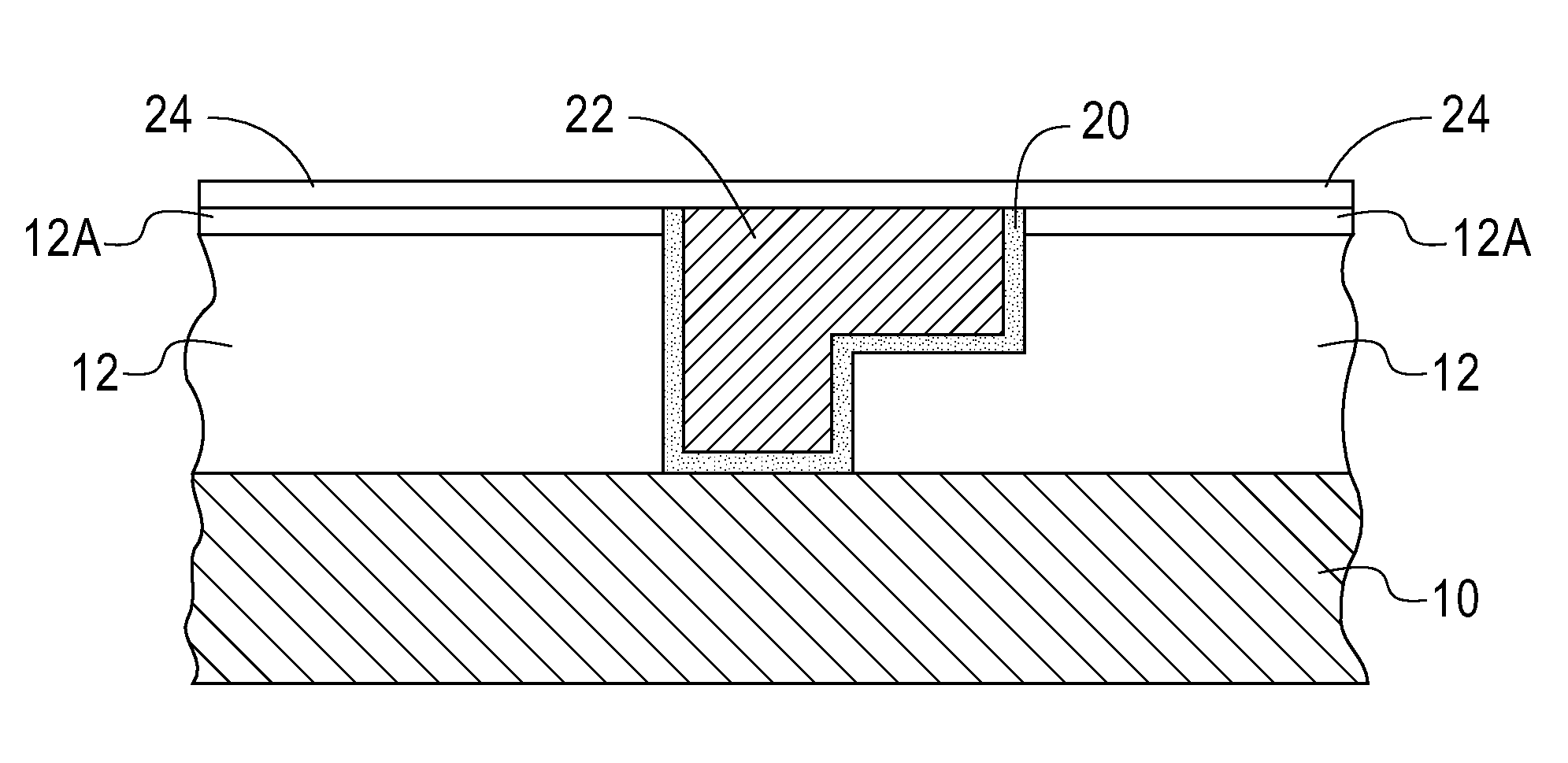
[0042]Reference is made to FIGS. 5A-5E which illustrate the processing steps of the first embodiment of the present invention for fabricating a reliable BEOL interconnect structure. Specifically, FIGS. 5A-5E shows cross sectional views of the interconnect structure through the various processing steps.

[0043]The first embodiment of the present invention, as shown in FIG. 5A, begins by first forming a ULK dielectric material 12 on a surface of a substrate 10. The term ‘substrate’ is used in the present application to include a semiconducting material, an insulating material, a conductive material or any combination thereof, including multilayered structures. Thus, for example, substrate 10 can be a semiconducting material such as Si, SiGe, SiGeC, SiC, GaAs, InAs, InP and other III / V or II / VI compound semiconductors. The semiconductor substrate 10 can also include a layered substrate such as, for example, Si / SiGe, Si / SiC, silicon-on-insulators (SOIs) or silicon germanium-on-insulators ...

second embodiment

[0073]In addition to the embodiment described above and illustrated in FIGS. 5A-5E, the present invention also contemplates a second embodiment in which the UV exposure step described in the first embodiment is replaced with a step of exposing the CMP processed ULK dielectric 12 shown in FIG. 5C to a chemical repair step including, for example, silylation. When silylation is employed a compound that is capable of silylating the CMP processed ULK dielectric such as a silane is employed. In this embodiment, gradient layer 12A is a hydrophobic surface such as a silylating surface that reacts with the Si—O groups formed during CMP. The hydrophobic surface can be formed by spin-on coating or a supercritical CO2 tool.

third embodiment

[0074]The present invention also provides a third embodiment which is similar to the first embodiment except that an additional UV exposure step is performed though the capping layer 24. Hence, in the third embodiment of the present invention, the structure shown in FIG. 5E is first provided as described above in the first embodiment, and then an additional UV exposure step using the same or different conditions as the UV exposure step in the first embodiment is employed. Note that the UV exposure process used in this embodiment must penetrate through the capping layer 24. In this embodiment, any plasma damage caused by the PPFCC step is repaired.

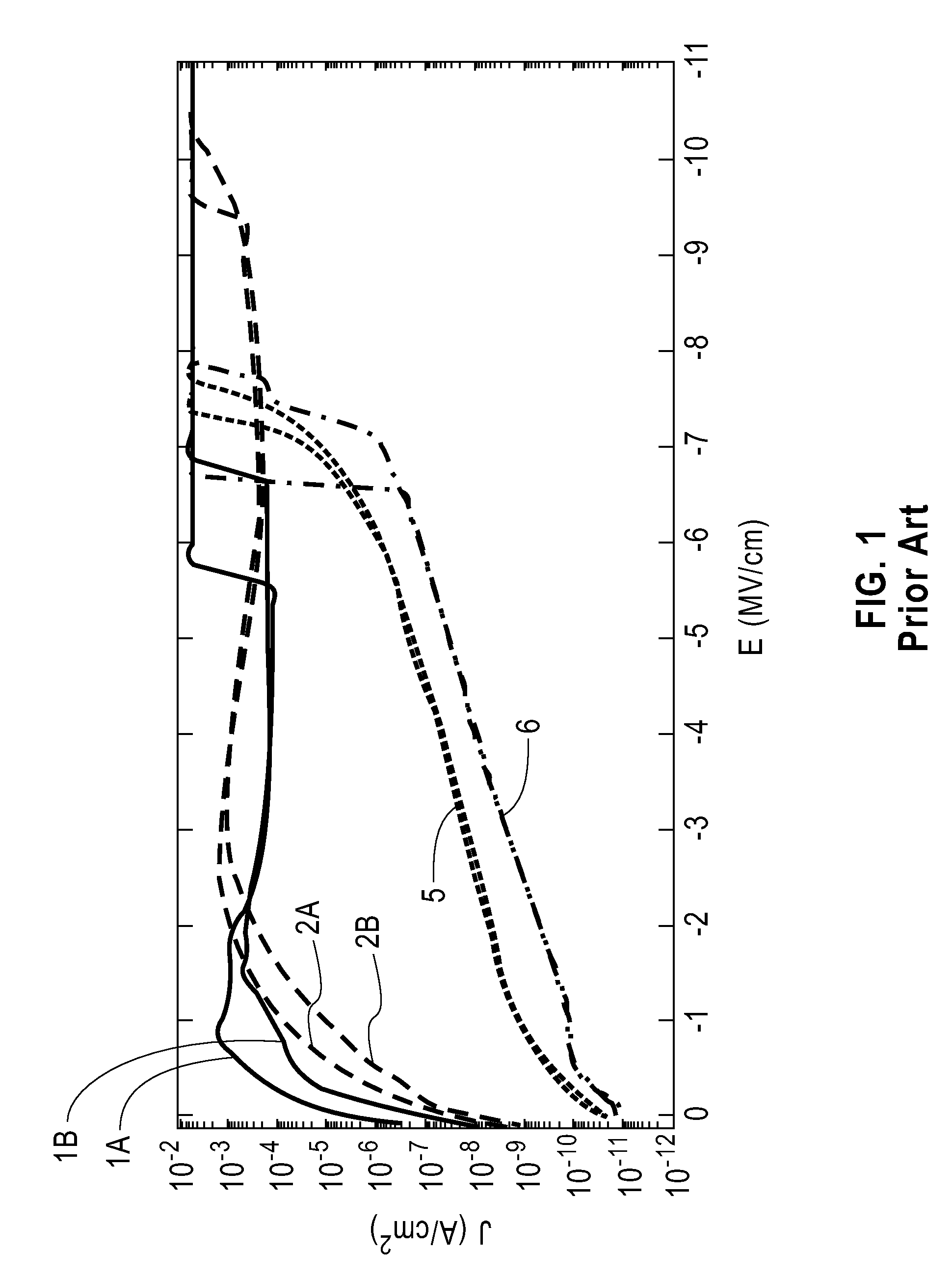
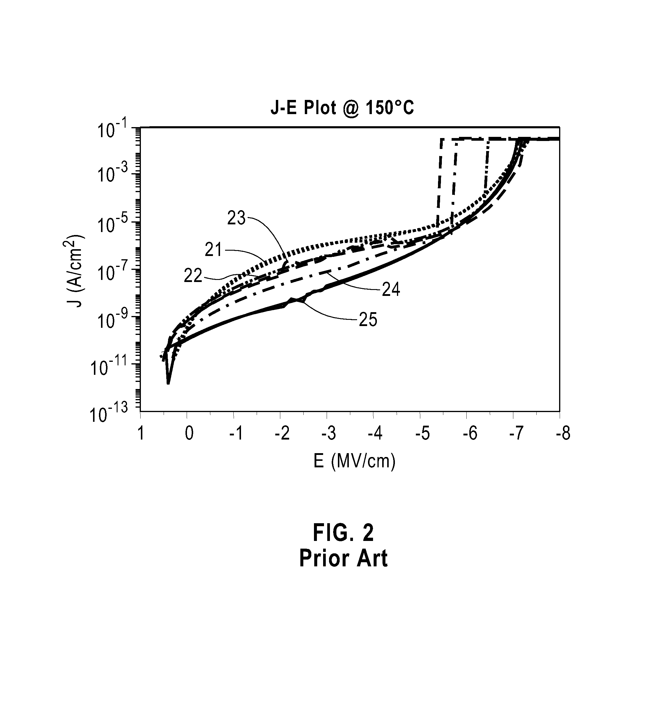
[0075]Of the various embodiments mentioned above, the first and third embodiments are preferred. Although the first and third are preferred over the second, each of the three embodiments provides an interconnect structure that is more reliable and has a lower conductivity between conductive layers, e.g., Cu lines, than the interconnect stru...


PUM

PropertyMeasurementUnit
dielectric constantaaaaaaaaaa
temperatureaaaaaaaaaa

Abstract

The present invention relates to methods of improving the fabrication of interconnect structures of the single or dual damascene type, in which there is no problem of hard mask retention or of conductivity between the metal lines after fabrication. The methods of the present invention include at least steps of chemical mechanical polishing and UV exposure or chemical repair treatment which steps improve the reliability of the interconnect structure formed. The present invention also relates to an interconnect structure which include a porous ultra low k dielectric of the SiCOH type in which the surface layer thereof has been modified so as to form a gradient layer that has both a density gradient and a C content gradient.

Description

FIELD OF THE INVENTION[0001]The present invention generally relates to integrated circuits (ICs). More particularly, the present invention relates to interconnect structures, including multilevel metal interconnect structures fabricated by damascene methods in which the capacitance and conductivity between metal lines is low. The present invention provides various methods for making improved interconnect structures based on metal damascene wiring having a reduced capacitance and stable, low, conductivity between metal lines, both during IC operation and reliability stress of the IC device.BACKGROUND OF THE INVENTION[0002]Generally, semiconductor devices include a plurality of circuits, which form an IC fabricated on a single silicon crystal substrate. A complex network of signal paths will normally be routed to connect the circuit elements distributed on the surface of the substrate. Efficient routing of these signals across the device requires the formation of multi-level or multi-...

Claims


Application Information

Patent Timeline
Patent Type & Authority Patents(United States)
IPC IPC(8): H01L21/44
CPCH01L21/76825H01L21/76826H01L21/76828H01L21/76829H01L21/76834H01L23/53295H01L2924/0002H01L21/76885H01L2924/00
Inventor DIMITRAKOPOULOS, CHRISTOS D.GATES, STEPHEN M.MCGAHAY, VINCENT J.MEHTA, SANJAY C.
Owner GLOBALFOUNDRIES INC
Why Eureka
Try Eureka