Method of fabricating alignment layer for liquid crystal display device
- Summary
- Abstract
- Description
- Claims
- Application Information
AI Technical Summary
Benefits of technology
Problems solved by technology
Method used
Image
Examples
Embodiment Construction
[0032]Reference will now be made in detail to the embodiments of the present invention, examples of which are illustrated in the accompanying drawings.
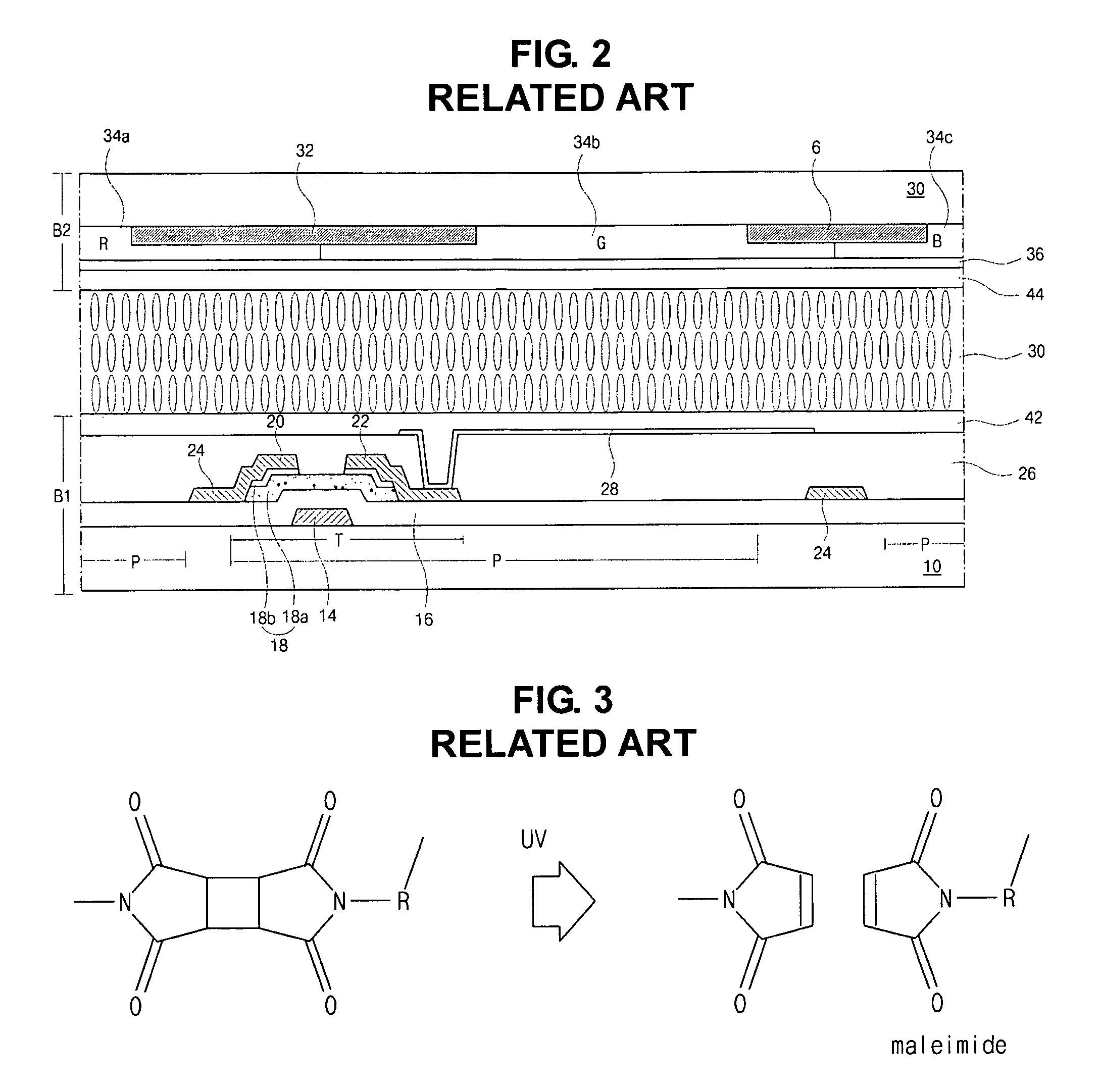
[0033]An alignment material for a method of fabricating an alignment layer includes a polyimide resin having a cyclobutane dianhydride (CBDA) ring of FIG. 3. A method for obtaining an alignment layer having improved properties is explained with FIGS. 6A to 6C.
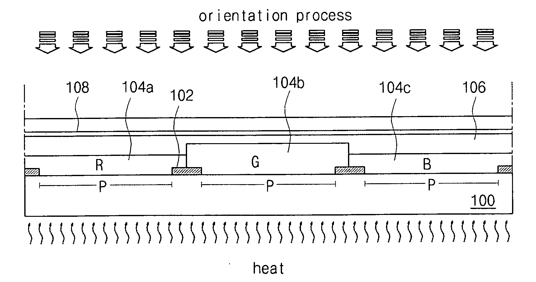
[0034]FIGS. 6A to 6C show fabricating processes of a color filter substrate having an alignment layer according to the present invention.
[0035]First, in FIG. 6A, a black matrix 102 is formed on a substrate 100 having a plurality of pixel regions P. The black matrix 102 has a lattice shape corresponding to each pixel region P. Although not shown, an LCD device has a counter substrate. On the counter substrate, a gate line, a data line and a thin film transistor are formed, and the black matrix 102 corresponds to them. Next, red (R), green (G) and blue (B) color filter patterns 102...
PUM
| Property | Measurement | Unit |
|---|---|---|
| Surface energy | aaaaa | aaaaa |
| Area | aaaaa | aaaaa |
| Area | aaaaa | aaaaa |
Abstract
Description
Claims
Application Information


