Method for fabricating master stamper/imprinters for patterned recording media utilizing hybrid resist

a technology of hybrid resist and recording media, which is applied in the direction of photomechanical equipment, photosensitive material processing, instruments, etc., can solve the problems of loss of stored information, adversely affecting the realization of ultra-high areal density data/information storage, and extremely minute recording bit sizes of continuous film media

Inactive Publication Date: 2008-05-15
SEAGATE TECH LLC
View PDF25 Cites 26 Cited by
  • Summary
  • Abstract
  • Description
  • Claims
  • Application Information

AI Technical Summary

Benefits of technology

[0026]An advantage of the present invention is an improved method of fabricating a master stamper / imprinter for use in manufacturing a patterned recording medium by means of nano-imprint lithography.
[0027]Another advantage of the present invention is an improved method of fabricating a master stamper / imprinter for use in manufacturing bit patterned recording media, track patterned recording media, and servo patterned recording media by means of nano-imprint lithography.
[0028]A further advantage of the present invention is improved master stampers / imprinters for use in manufacturing various types of patterned recording media by means of nano-imprint lithography.
[0029]Additional advantages and other aspects and features of the present invention will be set forth in the description which follows and in part will become apparent to those having ordinary skill in the art upon examination of the following or may be learned from the practice of the present invention. The advantages of the present invention may be realized and obtained as particularly pointed out in the appended claims.
[0030]According to an aspect of the present invention, the foregoing and other advantages are obtained in part by an improved method of fabricating a master stamper / imprinter for use in manufacturing a patterned recording medium by means of nano-imprint lithography, comprising steps of:
[0032](b) forming a layer of a hybrid resist material on the substrate surface, the hybrid resist layer having an exposed upper surface;

Problems solved by technology

Such conventional magnetic disk storage media based upon continuous magnetic recording films or layers incur a significant drawback / disadvantage which adversely affects realization of ultra-high areal density data / information storage.
As a consequence, recording bit sizes of continuous film media have become extremely minute, e.g., on the order of nanometers (nm).
However, the magnetization quantity of such minute bits is extremely small, resulting in a loss of stored information due to magnetization reversal by “thermal fluctuation”, also known as the “superparamagnetic effect”.
The superparamagnetic effect is a major limiting factor in increasing the areal recording density of continuous film magnetic recording media.
Superparamagnetism results from thermal excitations which perturb the magnetization of grains in a ferromagnetic material, resulting in unstable magnetization.
As the grain size of magnetic media is reduced to achieve higher areal recording density, the superparamagnetic instabilities become more problematic.
The superparamagnetic effect is most evident when the grain volume V is sufficiently small such that thermal energy demagnetizes the individual magnetic grains and the stored data bits are no longer stable.
Consequently, as the magnetic grain size is decreased in order to increase the areal recording density, a threshold is reached at which stable data storage is no longer possible.
However, a drawback associated with each of these techniques is formation of topographical patterns in the surface of the media, engendering media performance concerns such as transducer head flyability and corrosion, e.g., due to uneven lubricant thickness and adhesion.
Although e-beam lithography can produce extremely high resolution patterns, the throughput rates of available e-beam processing apparatus are typically very low, since e-beams must be directed to each location on the resist surface in sequence.
Unfortunately, however, for the reasons given above, resolution and product throughput rate are mutually competing characteristics of e-beam lithographic processing.
Increased resolution is achieved with a prohibitively high increase in e-beam writing times for large area substrates / workpieces (e.g., 95 mm diameter hard disks) and resultant low product throughput rates.

Method used


Image

  • Method for fabricating master stamper/imprinters for patterned recording media utilizing hybrid resist
  • Method for fabricating master stamper/imprinters for patterned recording media utilizing hybrid resist
  • Method for fabricating master stamper/imprinters for patterned recording media utilizing hybrid resist

Examples


Embodiment Construction

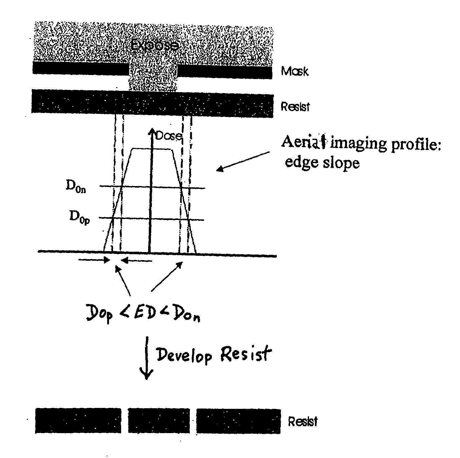
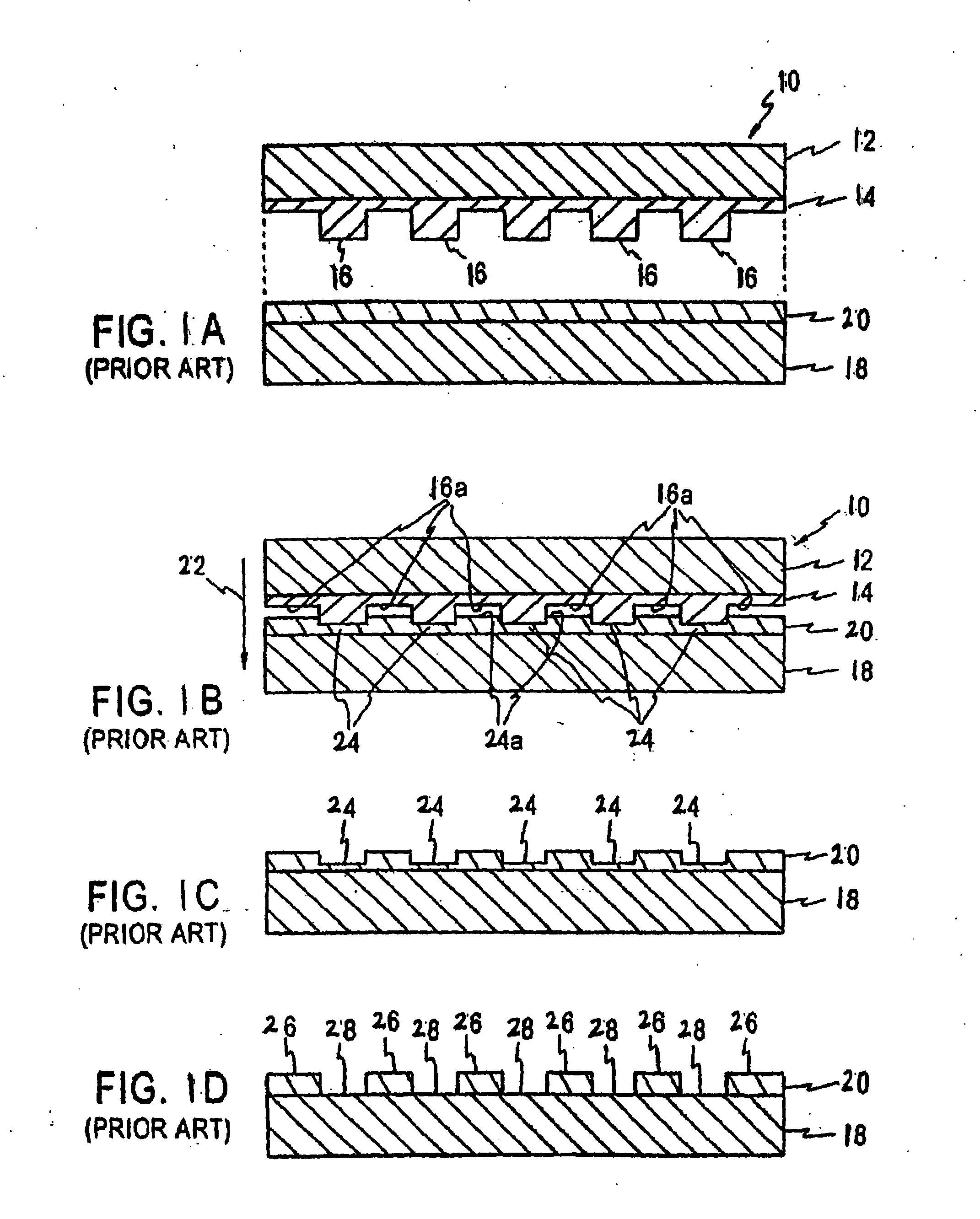
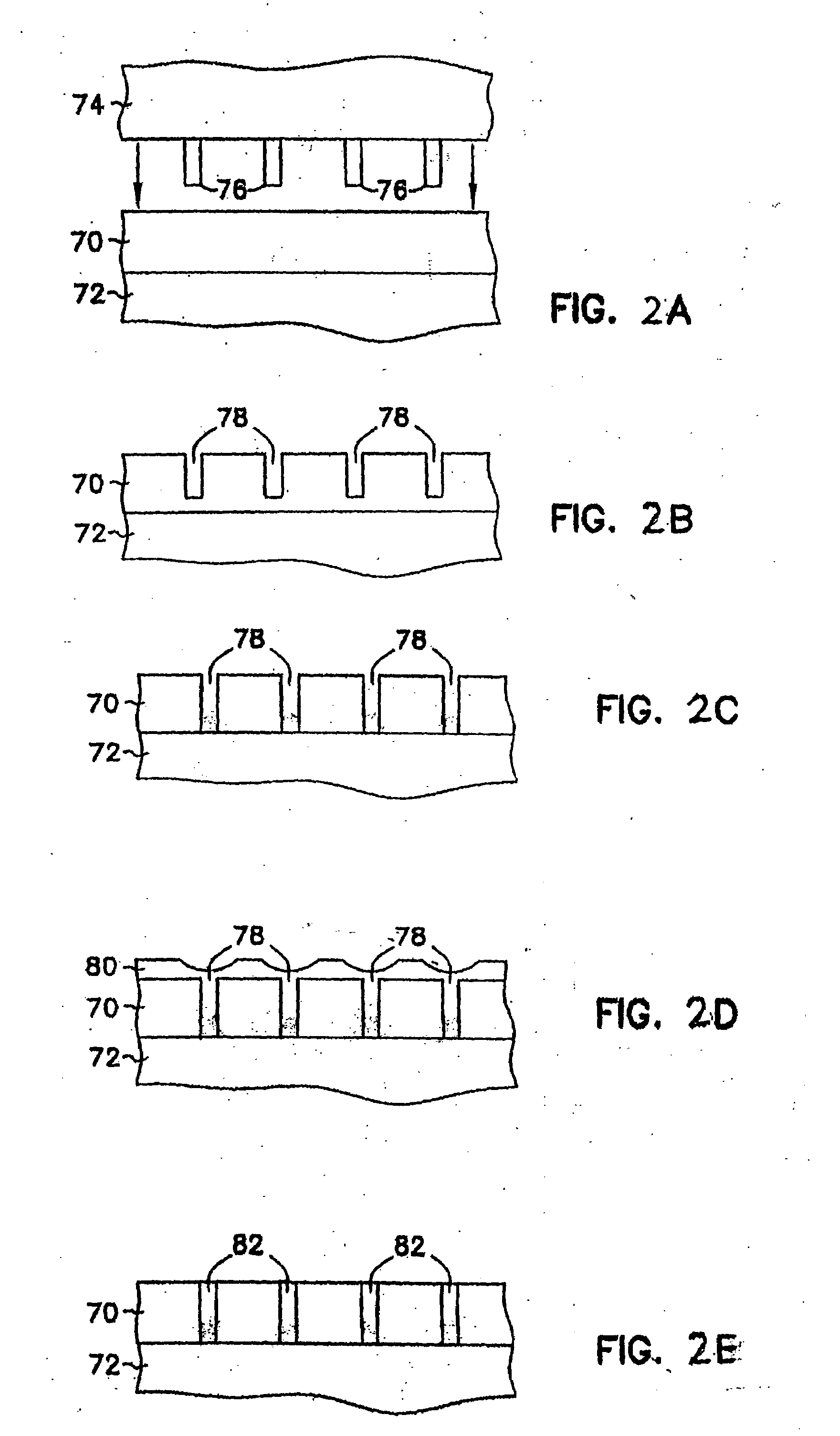
[0057]The present invention addresses and solves the above-described problems, disadvantages, and drawbacks associated with nano-imprint lithographic patterning methodologies utilized in the fabrication of master stamper / imprinters used in the manufacture of various types of patterned recording media, including, for example, bit, discrete track, and servo patterned hard disk magnetic media, while maintaining full capability with all aspects of automated manufacturing processing for formation of patterned media. Specifically, the inventive methodology addresses and solves the problem of low product throughput rate when performing high resolution e-beam processing for lithographic patterning of resist materials with ultra-small features necessitated by the requirement for further increase in areal recording density to the Tbit / in2 range. Advantageously, the inventive methodology can be practiced in a cost-effective manner without requiring capital-intensive processing techniques and i...


PUM

PropertyMeasurementUnit
depthsaaaaaaaaaa
diameteraaaaaaaaaa
energyaaaaaaaaaa

Abstract

A method of fabricating a master stamper / imprinter for manufacturing a patterned recording medium by nano-imprint lithography comprises steps of: (a) providing a substrate having a surface; (b) forming a layer of a hybrid resist material on the surface, the resist layer having an exposed upper surface; (c) subjecting selected areas of the exposed upper surface of the resist layer to an energy beam to form therein a latent image of a topographical pattern to be formed in the resist layer and having a correspondence to a pattern to be formed in a patterned recording medium; and (d) developing the latent image into the topographical pattern in the resist layer, wherein only those areas of the resist layer which have received an energy beam exposure dose between a positive-tone threshold dose D0p and a negative-tone threshold dose D0n are developed.

Description

FIELD OF THE INVENTION[0001]The present invention relates to an improved method for fabricating “master” stampers / imprinters utilized in the manufacture of patterned recording media and to the improved master stampers / imprinters obtained thereby. The invention enjoys particular utility in the manufacture of ultra-high areal recording density bit patterned magnetic media and servo patterned media, e.g., hard disk media utilized in computer-related applications.BACKGROUND OF THE INVENTION[0002]Designers, manufacturers, and users of electronic computers and computing systems require reliable and efficient equipment for storage and retrieval of information in digital form. Conventional storage systems, such as magnetic disk drives, are typically utilized for this purpose and are well known in the art. However, the amount of information that is digitally stored continually increases, and designers and manufacturers of magnetic recording media work to increase the storage capacity of magn...

Claims


Application Information

Patent Timeline
Patent Type & Authority Applications(United States)
IPC IPC(8): G03F7/00B32B3/00
CPCB82Y10/00B82Y40/00Y10T428/24355G03F7/0017G03F7/095G03F7/0002
Inventor LEE, KIM Y.WANG, HONG YINGLEE, SHIH-FUKUO, DAVID S.WAGO, KOICHIWELLER, DIETER K.
Owner SEAGATE TECH LLC
Why Eureka
Try Eureka