Optical scanner and image forming apparatus using optical scanner
an optical scanner and optical scanner technology, applied in the field of optical scanner and image forming apparatus, can solve the problems of optical properties, density irregularities on images, difference between magnification ratio changes,
- Summary
- Abstract
- Description
- Claims
- Application Information
AI Technical Summary
Problems solved by technology
Method used
Image
Examples
Embodiment Construction
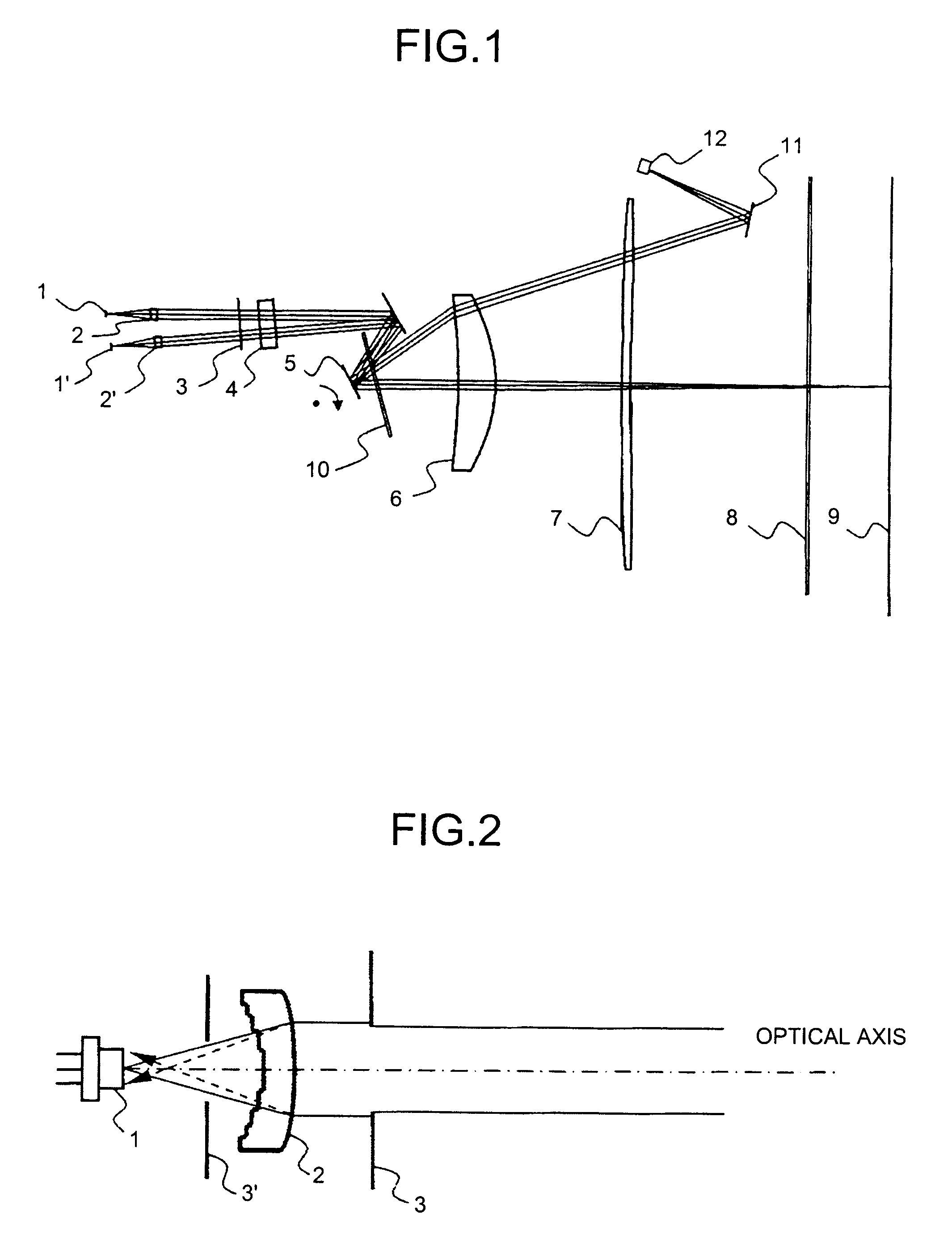
[0033]FIG. 1 is a schematic of a basic structure of an image forming apparatus according to the present invention.
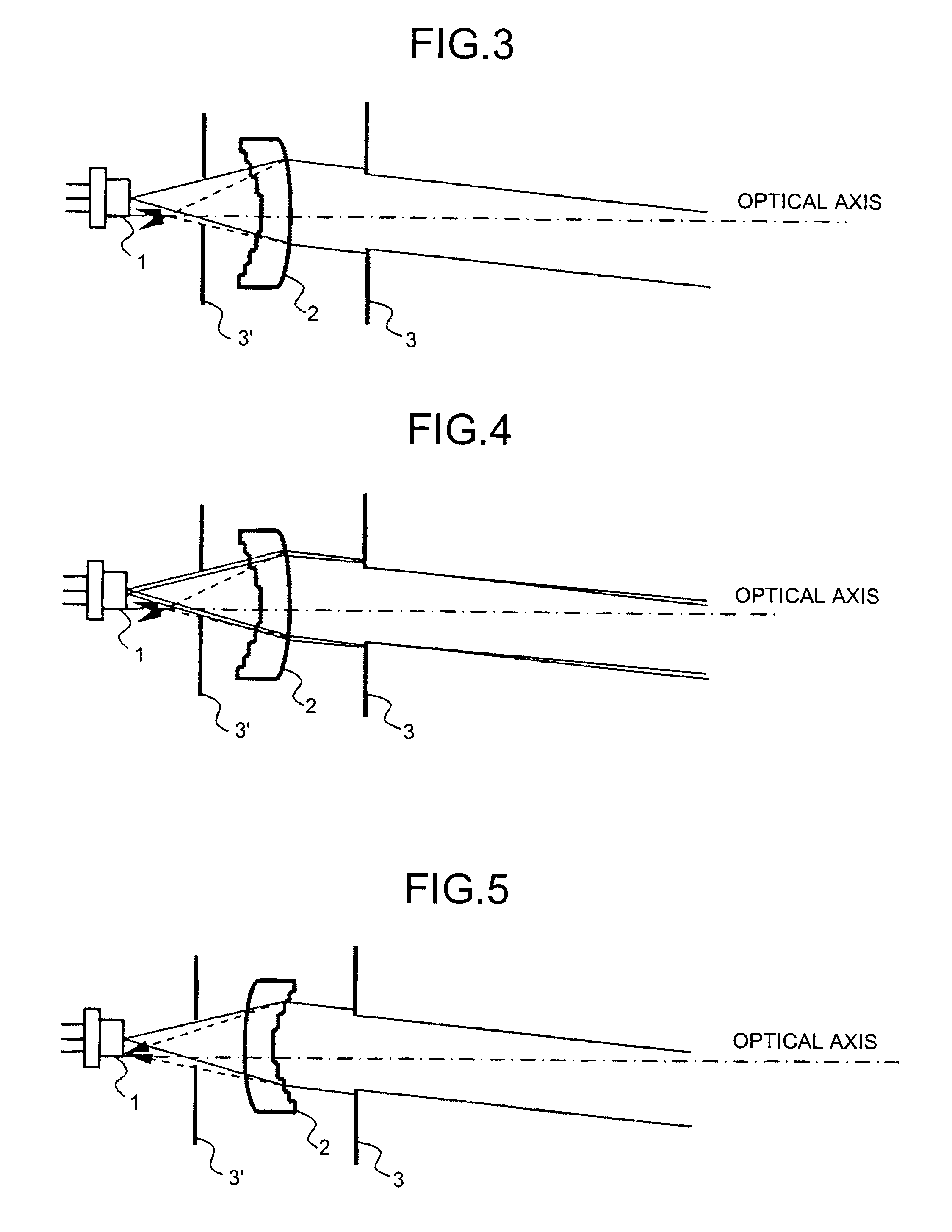
[0034]In FIG. 1, optical sources (semiconductor lasers) are denoted by 1 and 1′, coupling lenses (first lenses) are denoted by 2 and 2′, a first aperture is denoted by 3, an anamorphic lens (second lens) is denoted by 4, a polygon mirror as a deflector is denoted by 5, a deflector-side scanning lens is denoted by 6, an image-surface-side scanning lens is denoted by 7, a dust-proof glass is denoted by 8, an image surface is denoted by 9, a soundproof glass is denoted by 10, a synchronization mirror is denoted by 11, and a synchronization detector (photo detector) is denoted by 12.
[0035]The optical source 1 is a semiconductor laser having a cover glass of 0.3 mm in thickness.
[0036]A light beam emitted from the optical source 1 becomes a parallel light, a weak divergent light, or a weak convergent light via the coupling lens 2 having a resin-made diffracting surface. Subseq...
PUM
 Abstract
Description
Claims
Application Information


