Camera module having lower connection portions defining a chip region and engaging upper connection portions of a lens structure and method of fabricating the same

a technology of lens structure and connection portion, which is applied in the field of camera modules, can solve the problems of increasing fabrication cost, reducing yield, and difficult to miniaturize components, and achieves the effect of reducing the thermal budget of the bonding process

Active Publication Date: 2011-02-08
SAMSUNG ELECTRONICS CO LTD
View PDF12 Cites 13 Cited by
  • Summary
  • Abstract
  • Description
  • Claims
  • Application Information

AI Technical Summary

Benefits of technology

[0010]The present invention provides a method of fabricating a camera module that can reduce the thermal budget of a bonding process. Also, the present invention provides a method of fabricating a camera module without causing chipping or cracks. Furthermore, the present invention provides a camera module that is fabricated using a low-thermal-budget bonding process and without causing chipping or cracks.

Problems solved by technology

According to the conventional art, since the foregoing components are fabricated separately, it is difficult to miniaturize the components.
This technical restriction leads to the increase of the fabrication costs.
Furthermore, the image sensor chip is typically assembled while being exposed to atmosphere, thus causing a drop in yield due to particle contamination from the atmosphere.
However, even if the bonding process is performed at a low temperature, polymers may be deformed at the process temperature, thus resulting in the deformation of the lens structure.
However, due to the spacers having a high hardness property, technical problems, such as chipping and cracks, may be caused during the mechanical cutting process.

Method used


Image

  • Camera module having lower connection portions defining a chip region and engaging upper connection portions of a lens structure and method of fabricating the same
  • Camera module having lower connection portions defining a chip region and engaging upper connection portions of a lens structure and method of fabricating the same
  • Camera module having lower connection portions defining a chip region and engaging upper connection portions of a lens structure and method of fabricating the same

Examples


Embodiment Construction

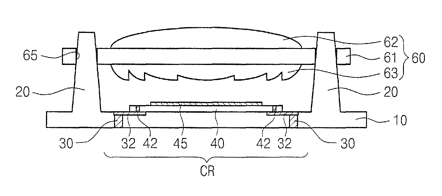
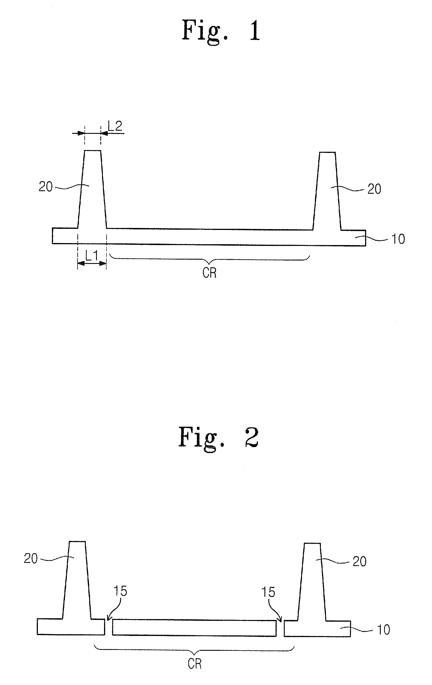
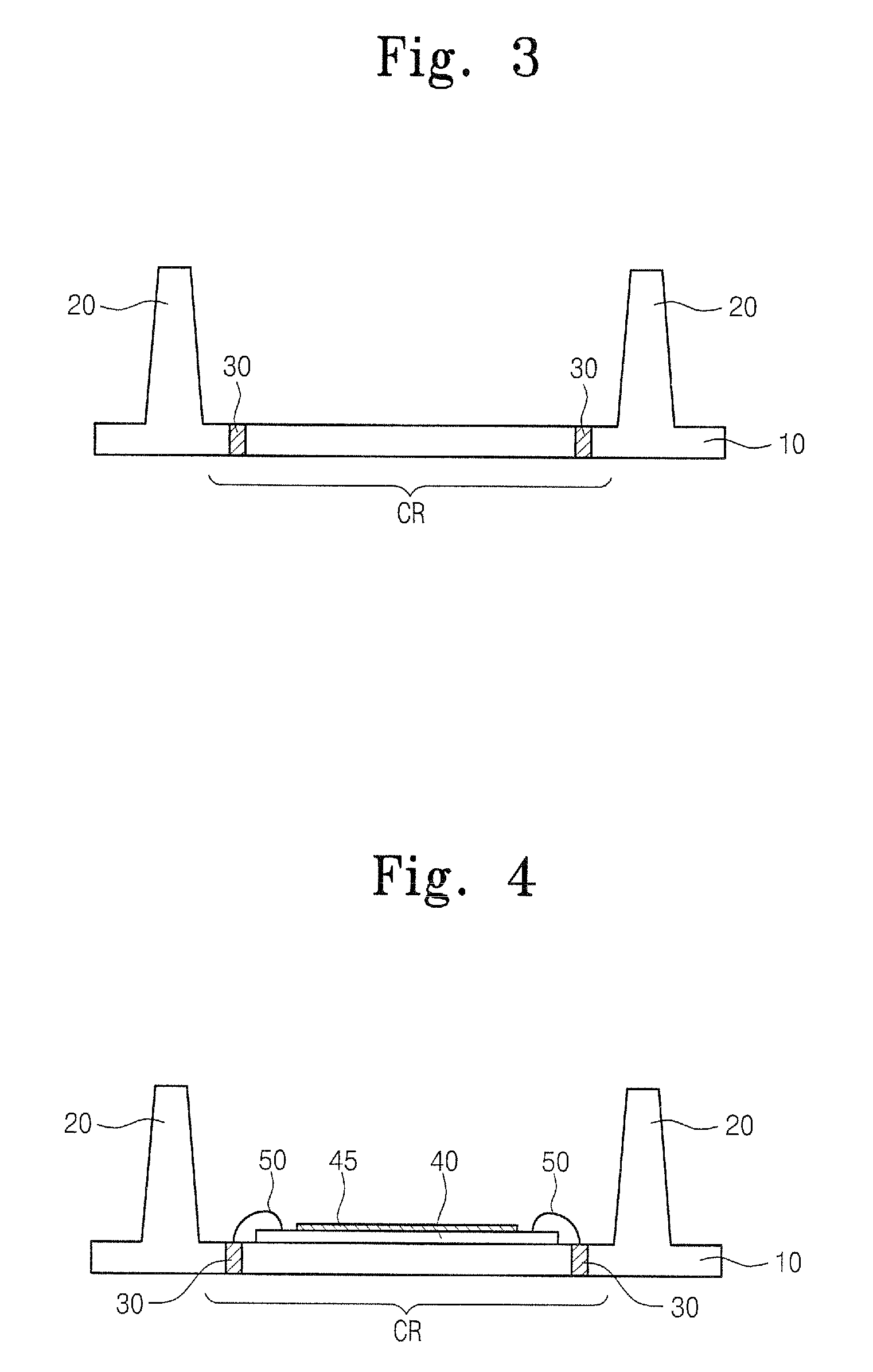
[0021]Reference will now be made in detail to the preferred embodiments of the present invention, examples of which are illustrated in the accompanying drawings. However, the present invention is not limited to the embodiments illustrated hereinafter, and the embodiments herein are rather introduced to provide easy and complete understanding of the scope and spirit of the present invention.

[0022]It will also be understood that when a layer is referred to as being “on” another layer or substrate, it can be directly on the other layer or substrate, or intervening layers may also be present. In the drawings, the thicknesses of layers and regions are exaggerated for clarity. It will be understood that although the terms first and second are used herein to describe various regions, layers and / or sections the invention should not be limited by these terms. These terms are only used to distinguish one region, layer or section from another region, layer or section. Thus, for example, a firs...


PUM


Abstract

Provided are a camera module and a method of fabricating the same. The method includes preparing a lens structure including upper connection portions. Lower connection portions are formed in a predetermined region of a substrate. The lower connection portions define a chip region and fit in the upper connection portions, respectively. An image sensor chip is located on the bottom surface of the chip region. The lens structure is adhered to the substrate using the upper and lower connection portions.

Description

CROSS-REFERENCE TO RELATED APPLICATION[0001]This application claims priority under 35 USC §119 to Korean Patent Application No. 10-2006-0097471, filed on Oct. 3, 2006, the disclosure of which is hereby incorporated herein by reference in its entirety.BACKGROUND[0002]1. Technical Field[0003]The present invention relates to a camera module and a method of fabricating the same.[0004]2. Description of the Related Art[0005]In recent years, portable phones including digital cameras are becoming widely popular. A camera module used for most portable phones includes an optical lens and an image sensor that converts incident light passing through the optical lens into an electrical signal. The electrical signal converted by the image sensor is transmitted to an image signal processing unit (ISP) and output as an image signal.[0006]More specifically, incident light passes through the optical lens, a micro-lens and an RGB filter and is incident on a photodiode. The photodiode generates charges...

Claims


Application Information

Patent Timeline
Patent Type & Authority Patents(United States)
IPC IPC(8): H04N5/225H01L21/00
CPCH01L27/14618H01L27/14625H01L27/14685H04N5/2257H01L24/97H01L31/0203H01L31/0232H01L2224/48091H01L2924/00014H01L2224/48235H01L2924/12043H04N23/57H01L2924/00H01L27/146H04N23/00
Inventor KWON, YONG-CHAILEE, DONG-HO
Owner SAMSUNG ELECTRONICS CO LTD
Why Eureka
Try Eureka