Substrate processing apparatus and method of manufacturing semiconductor device

a technology of semiconductor devices and processing apparatus, which is applied in the direction of electrical apparatus, microwave heating, electric/magnetic/electromagnetic heating, etc., can solve the problems of bad influence on organic chemical materials, and achieve the effect of reducing the thermal budg

Inactive Publication Date: 2012-05-24
KOKUSA ELECTRIC CO LTD
View PDF4 Cites 19 Cited by
  • Summary
  • Abstract
  • Description
  • Claims
  • Application Information

AI Technical Summary

Benefits of technology

[0014]As a substrate processing apparatus and a method of manufacturing a semiconductor device are configured as described above, a substrate can be heated while reducing an increase in temperature of the substrate to reduce a thermal budget.

Problems solved by technology

However, when a thermal budget is accumulated during the heating, a bad influence may be exerted on the organic chemical material when a heat-sensitive material is formed on the substrate.

Method used


Image

  • Substrate processing apparatus and method of manufacturing semiconductor device
  • Substrate processing apparatus and method of manufacturing semiconductor device
  • Substrate processing apparatus and method of manufacturing semiconductor device

Examples


first embodiment

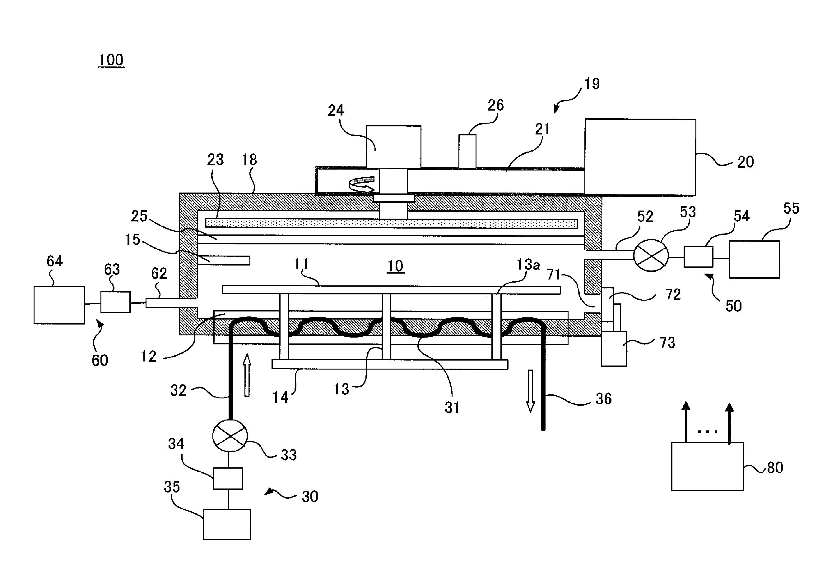
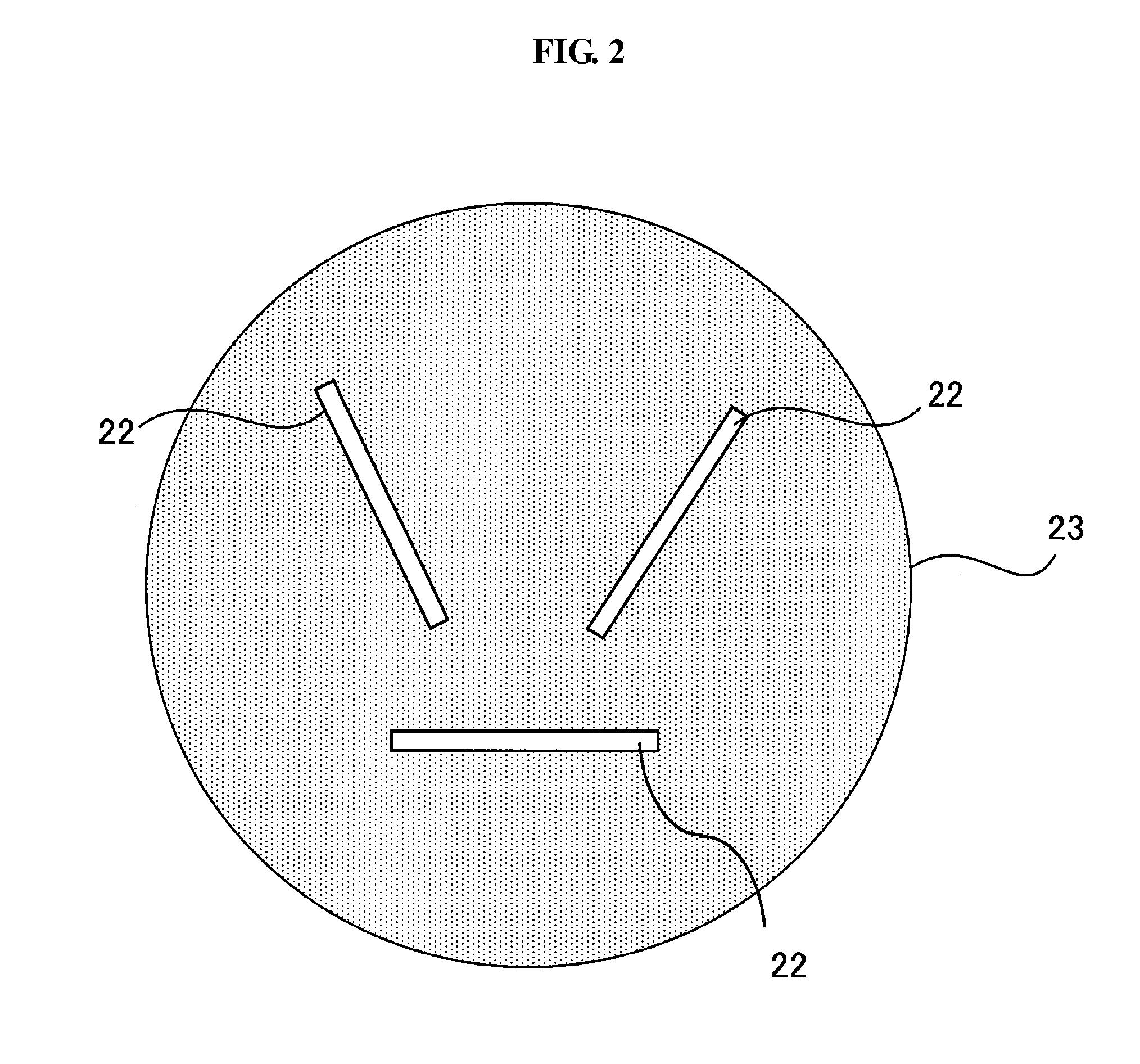
[0024]A configuration of a substrate processing apparatus in accordance with a first embodiment of the present invention will be described with reference to FIG. 1. FIG. 1 is a vertical cross-sectional view of the substrate processing apparatus in accordance with the first embodiment of the present invention. The substrate processing apparatus 100 includes a process chamber 10, a transfer chamber (not shown), and a microwave supply unit 19. The process chamber 10 processes a wafer 11, which is a semiconductor substrate. The microwave supply unit 19 includes a microwave generating unit 20, a waveguide 21, and a waveguide hole 22 (see FIG. 2).

[0025]

[0026]The microwave generating unit 20 generates, for example, fixed frequency microwaves. For example, a microtron, a klystron, or a gyrotron is used as the microwave generating unit 20. Microwaves generated from the microwave generating unit 20 are radiated into the process chamber from the waveguide hole 22 installed at a slot-type anten...

second embodiment

[0083]Next, a second embodiment will be described.

[0084]A type of an apparatus of the second embodiment uses substantially the same apparatus / process method as the first embodiment, except that the first position in the heating process is different.

[0085]In the second embodiment, the first position is located at a distance from 1 / 4 wavelength (λ / 4) of the microwaves or an odd multiple of λ / 4 from a surface facing the substrate support table 12 in the slot-type antenna 23 to maintain the wafer.

[0086]At this position, strength of the electric field of the microwaves on the substrate surface is maximized to enable effective irradiation of the microwave energy to the wafer surface.

[0087]In addition, in the invention, while the substrate is cooled on the substrate support table while rotating the slot-type antenna having a microwave supply hole and supplying the microwaves, the present invention is not limited thereto but may have a structure of relatively changing (for example, rotatin...


PUM


Abstract

Provided are a substrate processing apparatus and a method of manufacturing a semiconductor device that are capable of uniformly heating a substrate while reducing an increase in substrate temperature to reduce a thermal budget. The substrate processing apparatus includes a process chamber configured to process a substrate; a substrate support unit installed in the process chamber to support the substrate; a microwave supply unit configured to supply a microwave toward a process surface of the substrate supported by the substrate support unit, the microwave supply unit including a microwave radiating unit radiating the microwave supplied from a microwave source to the process chamber while rotating; a partition installed between the microwave supply unit and the substrate support unit; a cooling unit installed at the substrate support unit; and a control unit configured to control at least the substrate support unit, the microwave supply unit and the cooling unit.

Description

CROSS-REFERENCE TO RELATED PATENT APPLICATION[0001]This U.S. non-provisional patent application claims priority under 35 U.S.C. §119 of Japanese Patent Application No. 2010-258902, filed on Nov. 19, 2010, and No. 2011-151654, filed on Jul. 8, 2011, in the Japanese Patent Office, the entire contents of which are hereby incorporated by reference.BACKGROUND OF THE INVENTION[0002]1. Field of the Invention[0003]The present invention relates to a substrate processing technique for manufacturing a semiconductor device such as an integrated circuit (IC) on a substrate, and more particularly, to a semiconductor manufacturing apparatus for manufacturing a semiconductor device by processing a substrate such as a semiconductor wafer (hereinafter referred to as a “wafer”) using microwaves, a substrate processing apparatus for processing the substrate, and a method of manufacturing the semiconductor device.[0004]2. Description of the Related Art[0005]One semiconductor manufacturing process, a che...

Claims


Application Information

Patent Timeline
Patent Type & Authority Applications(United States)
IPC IPC(8): H01L21/26H05B6/80
CPCH01L21/67109H05B6/806H01L21/6875H01L21/67115H01L21/268H01L21/3105H01L21/324
Inventor OGAWA, UNRYUOKUNO, MASAHISAAKAO, TOKUNOBUYASHIMA, SHINJIUMEKAWA, ATSUSHIMINAMI, KAICHIRO
Owner KOKUSA ELECTRIC CO LTD
Why Eureka
Try Eureka