Semiconductor device and method for fabricating the same

a technology of semiconductor devices and semiconductor components, applied in the direction of semiconductor devices, electrical equipment, transistors, etc., can solve the problems of reduced area allocated for forming semiconductor devices, reduced distance between adjacent sources and drains, and inability to operate properly, etc., to reduce the needless thermal budget, reduce the distance between source junctions and drain junctions, and accelerate the thermal process

Inactive Publication Date: 2006-06-06
SAMSUNG ELECTRONICS CO LTD
View PDF8 Cites 3 Cited by
  • Summary
  • Abstract
  • Description
  • Claims
  • Application Information

AI Technical Summary

Benefits of technology

[0008]The present invention provides a semiconductor device and a method for fabricating the same so as to attain excellent electrical characteristics of MOS transistor devices by efficiently preventing a junction short circuit between sources and drains in a bulk area even if a channel distance between the sources and drains is reduced due to the high integration of devices.
[0012]It is preferable that the buried insulating layer is formed by chemical vapor deposition (CVD) to reduce thermal budget on the semiconductor substrate.
[0015]Preferably, the field oxide layer is formed to protrude from the surface of the semiconductor substrate to a predetermined height in order to perform as a mask pattern when selectively forming an epitaxial layer on the silicon substrate in the active region. In addition, the overgrowth over the field oxide layer can be prevented. Furthermore, the field oxide layer can be used as a polishing stopper when performing CVD after the overgrowth of epitaxial silicon.
[0023]Thereafter, impurity ions are implanted by using the gate structures as a mask, and the impurity ions are activated by using a predetermined thermal process to form source / drain junctions. Here, in the case of a PMOS transistor, P-type elements, such as boron (B) and boron fluoride (BF2), are implanted as the impurity ions. In the case of an NMOS transistor, N-type elements, such as phosphorus (P), arsenic (As), and antimony (Sb), are implanted as the junction ions. It is preferable that a rapid thermal process is used to reduce needless thermal budget on the semiconductor substrate, in order to form shallow junctions.
[0024]In the semiconductor device according to the present invention, a junction isolation insulating layer is formed under a channel, which connects a source and a drain arranged under a gate of a MOS transistor. Thus, the junction isolation insulating layer isolates a source junction and a drain junction. As a result, even when the distance between the source junction and the drain junction is reduced due to the reduction of a line width of the device, a short circuit due to the lateral diffusion or junction expansion of the junctions can be prevented.

Problems solved by technology

As a result, the areas allocated for forming semiconductor devices are also reduced, causing various problems in forming devices such as transistors.
When the devices are highly integrated, a short circuit can occur between source / drain junctions in a bulk region formed under channels, as well as a short channel effect, and the transistor devices may not operate properly.
However, as the devices have become more highly integrated and the design rule is extremely reduced, the distance between adjacent source and drain has become less than a critical value, even when the shallow junction method is used.
Consequently, junction areas are extended undesirably in the lateral direction.

Method used


Image

  • Semiconductor device and method for fabricating the same
  • Semiconductor device and method for fabricating the same
  • Semiconductor device and method for fabricating the same

Examples


first embodiment

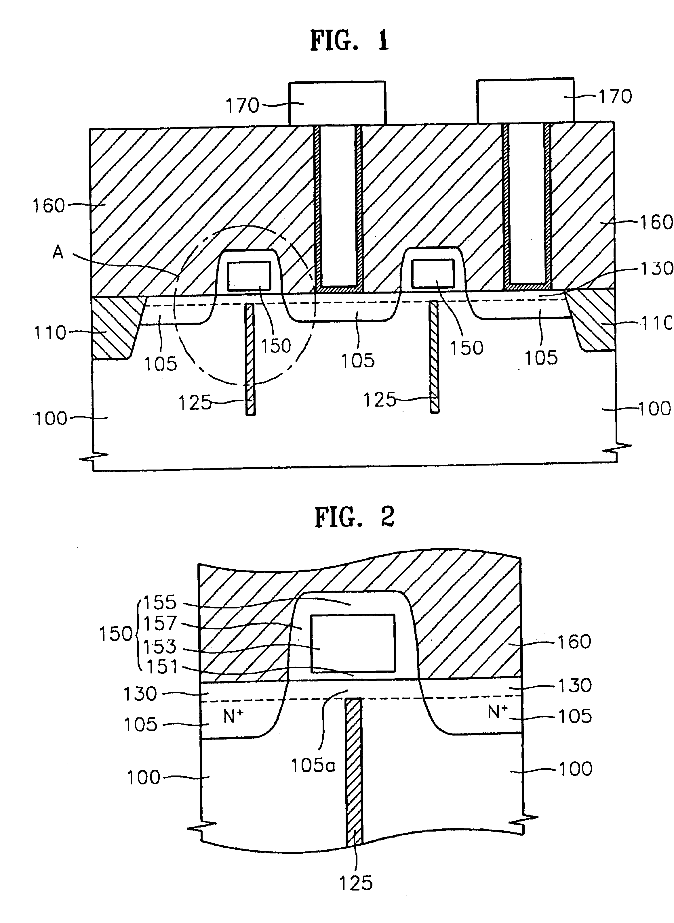
[0031]FIG. 1 is a cross-sectional view illustrating a semiconductor device according to the present invention, and FIG. 2 is a cross-sectional view illustrating portion A of FIG. 1.

[0032]Referring to FIGS. 1 and 2, a field oxide layer 110 (a field region) is formed in a semiconductor substrate such as a silicon substrate 100 to define an active region therebetween. Gate structures 150 are formed on the active region. The gate structures 150 include a gate insulating layer 151, a gate conductive layer 153, and a mask insulating layer 155. Further, sidewall spacers such as insulating spacers 157 can be formed on the sidewalls of the gate structures 150. Also, junction isolation insulating layers 125 are formed under the gate structures 150 to isolate source regions from drain regions in the active region with respect to the gate structures 150.

[0033]Further, an epitaxial silicon layer 130 extends above the upper portion of the silicon substrate 100 in the active region and also above ...

second embodiment

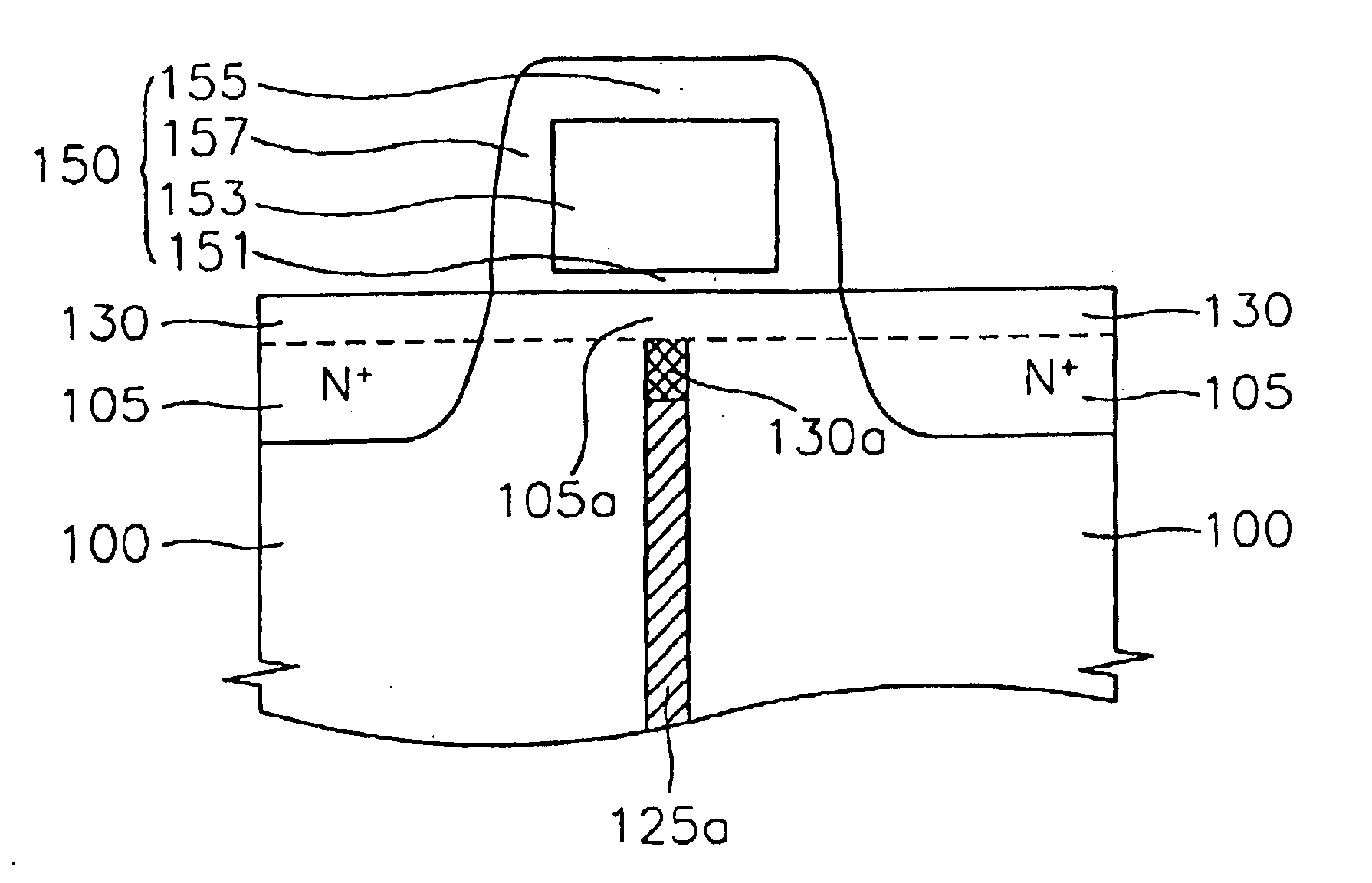
[0057]FIG. 10 is a sectional view illustrating a semiconductor device according to the present invention.

[0058]Referring to FIG. 10, junction isolation trenches 125a buried to a predetermined depth are not completely filled with an insulating material. In addition to the insulating material, the junction isolation trenches 125a are also filled with an epitaxial silicon layer 130. Accordingly, when the epitaxial silicon is grown, the epitaxial silicon at the sidewalls of the junction isolation trenches 125a is grown at the same time so that polysilicon 130a is grown in the junction isolation trenches 125a and the epitaxial silicon is grown at portions contacting the silicon substrate 100. Therefore, the characteristics of the epitaxial silicon layer 130 in channel regions 105a are improved, thereby improving the electrical characteristics of the semiconductor device.

[0059]A semiconductor device and a method for fabricating the same according to the present invention provides the foll...


PUM


Abstract

A semiconductor device and a method for fabricating the same are provided. The provided semiconductor device includes a field oxide layer formed in a semiconductor substrate to define an active region; gate structures formed on the active region; source / drain junctions formed on either side of the gate structures on the semiconductor substrate; a channel silicon layer arranged under the gate insulating layer to operate as a channel for connecting sources and drains; and buried junction isolation insulating layers under the channel silicon layer. The buried junction isolation insulating layers isolate source / drain junction regions of a MOS transistor, so that a short circuit in a bulk region under the channel of a transistor due to the high-integration of the device can be prevented.

Description

BACKGROUND OF THE INVENTION[0001]This application claims priority from Korean Patent Application No. 2002-32974, filed Jun. 12, 2002, which is incorporated herein by reference in its entirety.[0002]1. Field of the Invention[0003]The present invention relates to semiconductor devices and a method for fabricating the same, and more particularly, to semiconductor devices having a structure where an epitaxial silicon layer is formed in an active region and sources and drains are formed in the epitaxial silicon layer and a fabricating method of the same.[0004]2. Description of the Related Art[0005]As semiconductor devices become more highly integrated, the design rule for the devices decreases. As a result, the areas allocated for forming semiconductor devices are also reduced, causing various problems in forming devices such as transistors. An NMOS transistor in a cell region having a memory device and PMOS and NMOS transistors in a peripheral region can secure electrical characteristic...

Claims


Application Information

Patent Timeline
Patent Type & Authority Patents(United States)
IPC IPC(8): H01L29/76H01L21/8238H01L27/092H01L21/336H01L21/761H01L21/8234H01L29/06H01L29/78
CPCH01L21/761H01L21/823412H01L21/823425H01L21/823878H01L29/0649H01L29/66651H01L21/823481H01L29/78H01L27/092
Inventor KIM, JI-YOUNGKIM, KI-NAM
Owner SAMSUNG ELECTRONICS CO LTD
Why Eureka
Try Eureka