Salicide process

a technology of salicide and process, applied in the direction of semiconductor devices, electrical devices, transistors, etc., can solve the problems of affecting the performance of the device, and affecting the operation of the device, so as to reduce the thermal budget of salicide processes, reduce the effect of agglomeration phenomenon, and increase sheet resistan

Inactive Publication Date: 2007-03-15
UNITED MICROELECTRONICS CORP
View PDF6 Cites 19 Cited by
  • Summary
  • Abstract
  • Description
  • Claims
  • Application Information

AI Technical Summary

Benefits of technology

[0013] In contrast to the conventional salicide process, the present invention aims to reduce the thermal budget of salicide processes when salicides are formed on the substrate. Consequently, the present invention is able to reduce the effects of the agglomeration phenomenon and increase in sheet resistance caused by an overly high temperature or prolonged treatment time, and at the same improve the spiking phenomenon in the ultra shallow junction and the problem of converting low resistivity nickel silicide (NiSi) to high resistivity nickel disilicide (NiSi2).

Problems solved by technology

Nevertheless, the interconnection between the contact plugs and the silicon material of the gate structure and the source / drain region is usually poor, hence a silicide material is often formed over the surface of the gate structure and the source / drain region to improve the ohmic contact between the contact plugs and the gate structure and the source / drain region.
However, when the silicides are being formed, the atoms within the metal layer will diffuse into the substrate and deplete the silicon within the source / drain region, thereby damaging the original lattice structure of the source / drain region and causing the PN junction between the source / drain region and the silicon substrate to react with the silicon contained within the source / drain region as a result of an overly short distance between the PN junction and the silicide layer.
Ultimately, the problems become much worse in the design of ultra shallow junctions (USJ) as the silicides often come in contact directly with the substrate and result in failure of the device.
On the other hand, if the depth of the silicides is kept constant, the distance between the PN junction of the source / drain region 112 and the silicon substrate and the silicide layer 116 may become overly short and result in junction leakage.
Additionally, the mixture utilized during the wet cleaning process will corrode the liner disposed between the gate electrode and the spacer and cause the silicide to approach the channel area during silicide formation and result in a nickel silicide piping phenomenon.
Moreover, due to high temperature of the PVD chamber or the degas process, the as-deposition formed before the rapid thermal annealing process will result in silicides with polycrystalline structure and degrade the overall thermal stability.
In other words, when the treatment temperature is too high or process time of the treatment is too long, the silicides will become pieces of unconnected mass and result in an agglomeration phenomenon and increase the sheet resistance.
Additionally, a high temperature will induce a conversion and consume silicon excessively, and cause a spiking phenomenon in the ultra shallow junction or forming a high resistivity structure, such as converting the low resistivity state nickel silicide (NiSi) having less than 20 μ, Ω-cm to a high resistivity state nickel disilicide (NiSi2) having approximately 50 μ, Ω-cm.

Method used


Image

  • Salicide process
  • Salicide process
  • Salicide process

Examples


Embodiment Construction

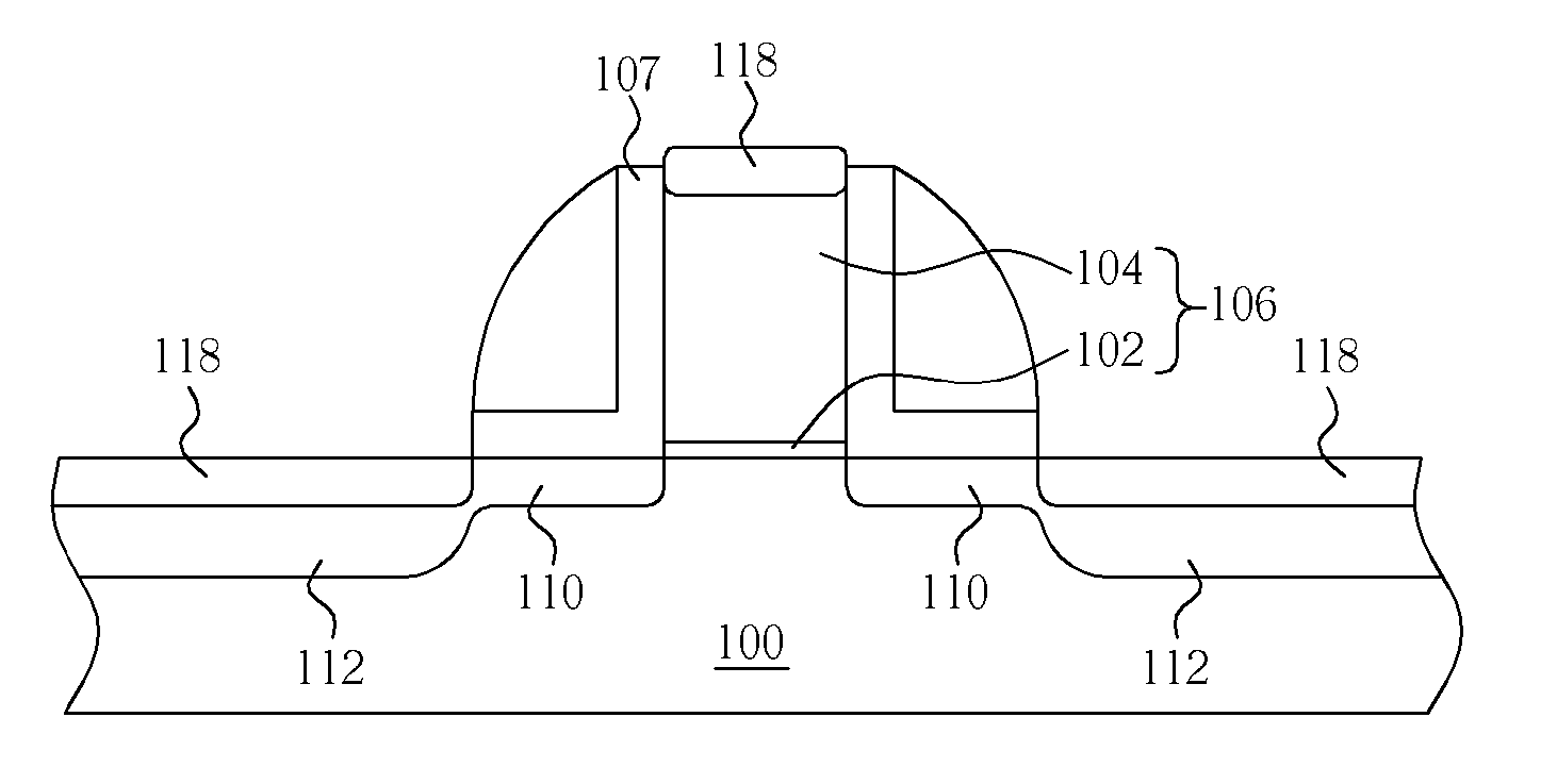
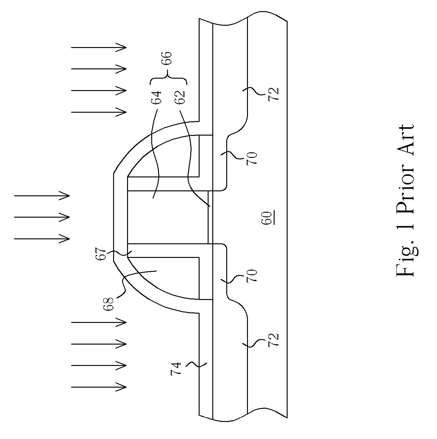
[0018] Please refer to FIG. 3 through FIG. 5. FIG. 3 through FIG. 5 are perspective diagrams showing the means of applying a salicide process to the fabrication of MOS transistors according to the present invention. As shown in FIG. 3, a substrate 100, such as a wafer or silicon-on-insulator (SOI) substrate is provided, in which the surface of the substrate 100 includes at least a silicon layer (not shown) composed of single crystal silicon, polysilicon, or epitaxial material. Preferably, the silicon layer may include structures such as gates, source / drain regions, word lines, or resistors depending on different product demands and fabrication processes. According to the preferred embodiment of the present invention, a gate structure 102 and source / drain region 112 of a MOS transistor are utilized as an example, as shown in FIG. 3 through FIG. 5. As shown in FIG. 3, the gate structure 102 includes a gate dielectric layer 102 and gate 104, in which the gate dielectric layer 102 is co...


PUM

PropertyMeasurementUnit
temperatureaaaaaaaaaa

Abstract

A salicide process includes providing a substrate, in which the surface of the substrate contains at least a silicon layer; performing a degas process on the substrate; performing a cooling process on the substrate; depositing a metal layer over the surface of the substrate, in which the surface of the metal layer and the surface of the silicon layer are in contact with each other; and removing the unreacted metal layer.

Description

BACKGROUND OF THE INVENTION [0001] 1. Field of the Invention [0002] The present invention relates to a method of fabricating semiconductor devices, and more particularly, to a method of performing salicide processes. [0003] 2. Description of the Prior Art[0004] Field effect transistors are important electronic devices in the fabrication of integrated circuits, and as the size of the semiconductor device becomes smaller and smaller, the fabrication of the transistors also improves and is constantly enhanced for fabricating transistors with smaller sizes and higher quality. [0005] In the conventional method of fabricating transistors, a gate structure is first formed on a substrate, and a lightly doped drain (LDD) is formed on the two corresponding sides of the gate structure. Next, a spacer is formed on the sidewall of the gate structure and an ion implantation process is performed to form a source / drain region within the substrate by utilizing the gate structure and spacer as a mask...

Claims


Application Information

Patent Timeline
Patent Type & Authority Applications(United States)
IPC IPC(8): H01L21/8238H01L21/44
CPCH01L21/28052H01L21/28518H01L29/7833H01L29/6656H01L29/6659H01L29/665
Inventor CHANG, YU-LANHSIEH, CHAO-CHINGCHIANG, YI-YIINGCHEN, YI-WEIHUNG, TZUNG-YULI, JIA-RUNG
Owner UNITED MICROELECTRONICS CORP
Why Eureka
Try Eureka