Method for assembling testing equipment for semiconductor substrate

a technology for semiconductor substrates and testing equipment, which is applied in the direction of individual semiconductor device testing, semiconductor/solid-state device testing/measurement, instruments, etc., can solve the problems of enormous assembly time, and achieve the effect of easy and accurate adjustment of the relative position of the probe pin

Inactive Publication Date: 2011-03-22
YAMAICHI ELECTRONICS
View PDF23 Cites 1 Cited by
  • Summary
  • Abstract
  • Description
  • Claims
  • Application Information

AI Technical Summary

Benefits of technology

[0016]In view of the above problems, an object of the present invention is to provide a method for assembling a testing equipment for a semiconductor substrate which is able to easily and accurately adjust the relative position of the probe pin in the contact block to the pitch-changing substrate.
[0020]As apparent from the above-mentioned explanation, according to the inventive method for assembling a testing equipment for a semiconductor substrate, since the step for making the positioning mark in the changing substrate to coincide with the mark detection hole in the contact block, which the positioning mark are formed in correspondence with the mark detection hole in the contact block to have a predetermined positional relationship to a position of the electrode group is comprised, it is possible to easily and accurately adjust the relative position of the probe pin in the contact block to the changing substrate.

Problems solved by technology

As a result, there may be a risk in that the adjustment of the positioning is many a time repeated to result in enormous amounts of the time required for the assembly.

Method used


Image

  • Method for assembling testing equipment for semiconductor substrate
  • Method for assembling testing equipment for semiconductor substrate
  • Method for assembling testing equipment for semiconductor substrate

Examples


first embodiment

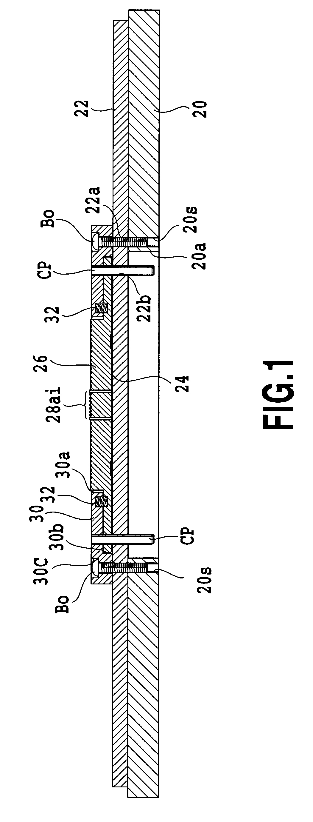
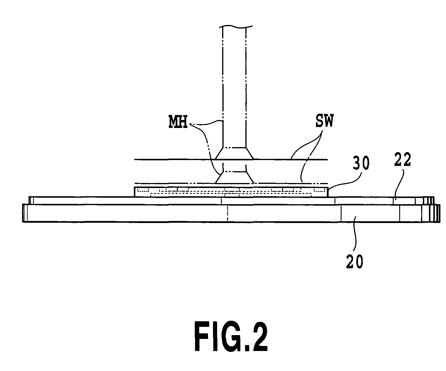
[0042]FIG. 2 schematically illustrates an overall structure of a probe head unit to which is applied the method for assembling a testing equipment for a semiconductor substrate in accordance with the present invention.

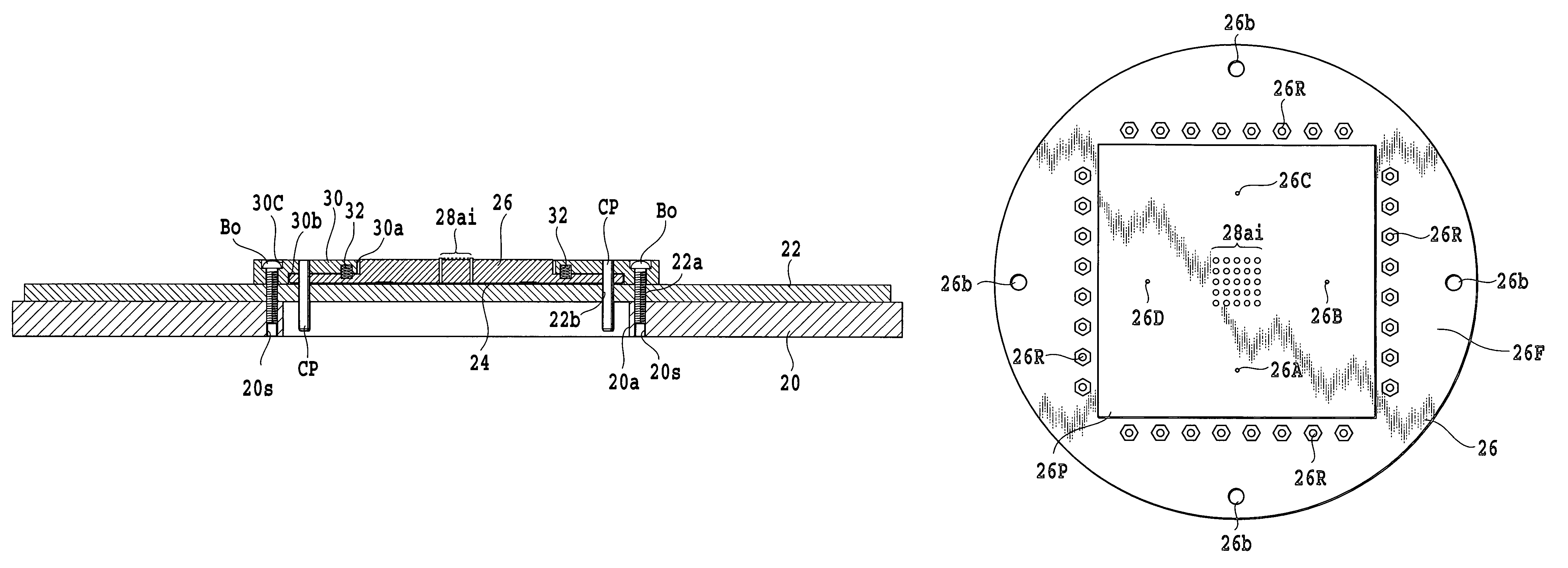
[0043]In FIG. 2, the probe head unit for the electric connection to a semiconductor substrate SW includes a reinforcement frame member 20 for reinforcing the rigidity of a printed wiring board 22, and a printed wiring board 22 as a test board for supplying test signals or others to circuit patterns in the tested semiconductor substrate SW disposed on one surface of the reinforcement frame member 20. As shown in FIG. 1, the probe head unit further includes a pitch-changing substrate 24 for the mutual electric connection between the printed wiring board 22 and a contact block 26 described later 26, the contact block 26 having a plurality of probe pins 28ai (i=1 to n, n is a positive integer) for the electric connection between the circuit patterns in the semiconductor su...

second embodiment

[0069]FIG. 9 schematically illustrates an overall structure of a probe head unit to which is applied the inventive method for assembling a testing equipment for a semiconductor substrate.

[0070]In the example shown in FIG. 1, the contact block 26 has the convex portion 26P and the flange portion 26F. Contrarily, in the example shown in FIG. 9, a contact block 36 has no such a flange portion, but, instead thereof, a dowel member 38 is disposed on the pitch-changing substrate 24. In this regard, in the example shown in FIG. 9 and examples shown in FIGS. 10 to 19 described later, the same reference numerals are used for denoting the same elements and the explanation thereof will be eliminated.

[0071]The contact block 36 has a plurality of probe pins 36ai (i=1 to n, n is a positive integer) generally at a center thereof in correspondence to an electrode group 24E in the pitch-changing substrate 24 described above. Opposite ends of the probe pin 36ai penetrating the center are projected fr...

third embodiment

[0089]FIG. 12 schematically illustrates an overall structure of a probe head unit to which is applied the inventive method for assembling a testing equipment for a semiconductor substrate.

[0090]In the example shown in FIG. 9, the opening 20a in the reinforcement frame member 20 is a vacant space. Contrarily, in the example shown in FIG. 12, a second reinforcement frame member 40 is disposed in this space in accordance with the rigidity of the printed wiring board 22. In this regard, in FIGS. 12 to 15, the same reference numerals are used for denoting the same elements as in FIG. 9, and the explanation thereof will be eliminated.

[0091]The reinforcement frame member 40 has holes 40a at positions directly beneath the respective holes 22b in the printed wiring board 22, into which are inserted one ends of the respective positioning pins CP1. Thus, the one ends of the positioning pins CP1 are inserted into the holes 40a to further increase the rigidity of the printed wiring board 22.

[009...


PUM

PropertyMeasurementUnit
widthaaaaaaaaaa
diameteraaaaaaaaaa
diameteraaaaaaaaaa

Abstract

Upon an assembly of a probe head unit, the relative positions of the probe pins 28ai to those of the electrode group 24E in the pitch-changing substrate 24 are determined by making the positions of the through-holes 26A, 26B, 26C and 26D in the contact block 26 to coincide with the positioning marks 24MA, 24MB, 24MC and 24MD in the pitch-changing substrate 24.

Description

[0001]This application claims priority from Japanese Patent Application Laid-open No. 2005-122840 filed Apr. 20, 2005 which is hereby incorporated by reference herein.BACKGROUND OF THE INVENTION[0002]1. Field of the Invention[0003]The present invention relates to a method for assembling a testing equipment for a semiconductor substrate.[0004]2. Description of the Related Art[0005]A semiconductor substrate, such as a silicon wafer, is tested by a testing equipment prior to a dicing process regarding a circuit pattern formed in the respective area thereof. Such a testing equipment is provided with a probe head unit movable to each of the areas, having probe pins to be in contact with the respective circuit pattern for delivering or receiving test signals thereto or therefrom as disclosed, for example, in Japanese Patent Application Laid-open No. 2000-321303.[0006]As shown in FIG. 20, the probe head unit includes a reinforcement frame member 2 for reinforcing the rigidity of a printed ...

Claims


Application Information

Patent Timeline
Patent Type & Authority Patents(United States)
IPC IPC(8): H01R43/00H05K3/10H01R43/16
CPCG01R31/31905G01R31/2886Y10T29/49155Y10T29/49222Y10T29/49204
Inventor SUZUKI, TAKEYUKIUJIKE, RYO
Owner YAMAICHI ELECTRONICS
Why Eureka
Try Eureka