
Method for performing a logic built-in-self-test in an electronic circuit

a logic and electronic circuit technology, applied in the field of methods for performing logic built-in self-tests on electronic circuits, can solve problems such as slow and costly process

Inactive Publication Date: 2011-03-22
IBM CORP
View PDF3 Cites 2 Cited by
  • Summary
  • Abstract
  • Description
  • Claims
  • Application Information

AI Technical Summary

Benefits of technology

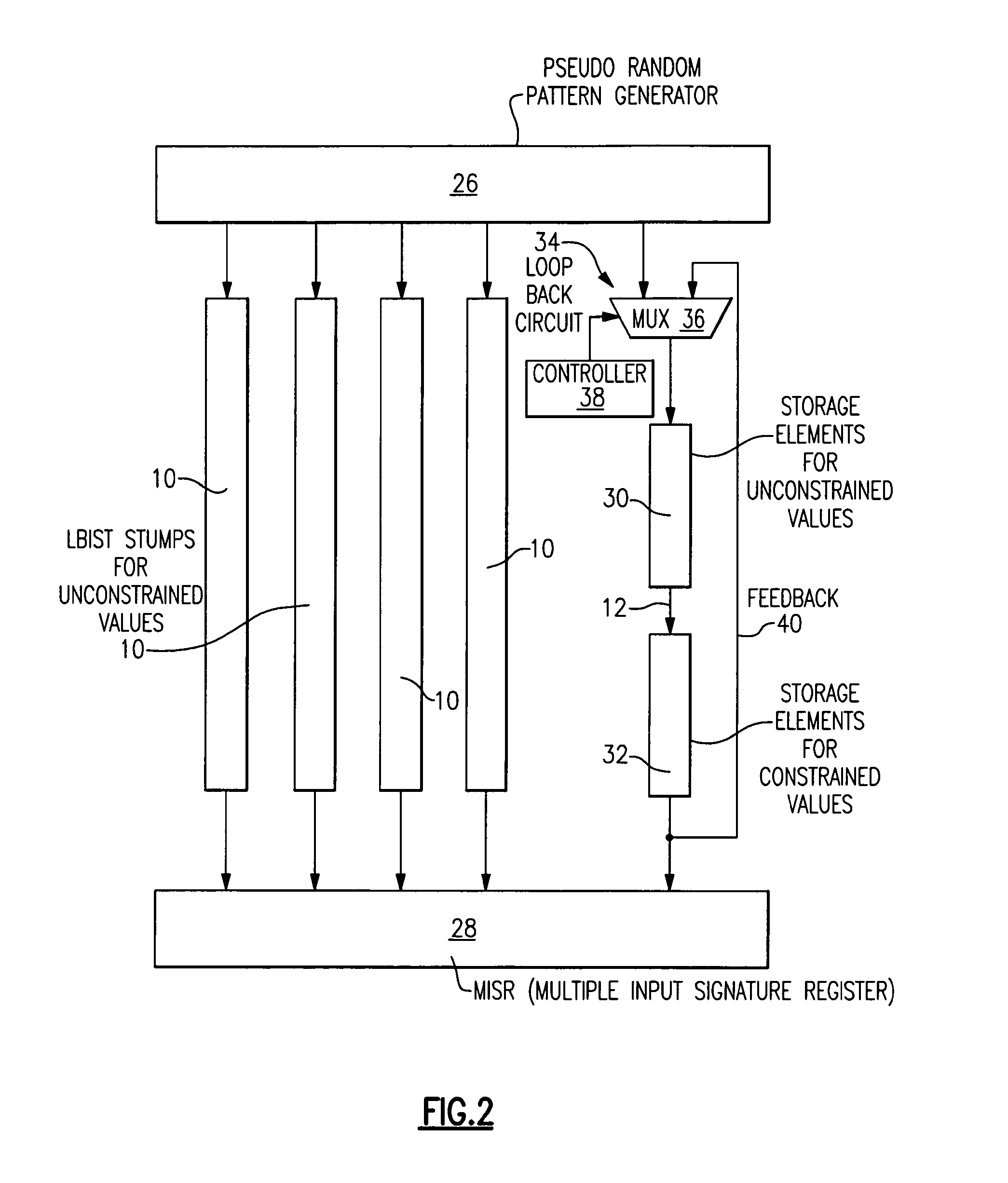
[0015]The scan process of the LBIST stumps is slightly modified in order to avoid overwriting the well-constrained data during the scan process. This can easily be achieved by a multiplexer that determines, whether the data from the pseudo-random-pattern generator (PRPG) are to be shifted into the LBIST stump or the output of the LBIST stump is to be looped back. The latter mode preserves the well-constrained data in the LBIST stump and can be used for the complete LBIST stump or only for a part of said LBIST stump as a function of a configuration register in the logic of the PRPG.
[0016]The method according to the present invention avoids the effort of generating manually designed patterns for the above case. It is not necessary to scan manual patterns into the chip from an external tester. This would be a very slow and costly process.
[0017]The present invention allows high fault coverage with a fully automatic LBIST. The required special logic can be seamlessly integrated with the random logic. The method according to the present invention allows a higher speed than manual test patterns. This is very advantageous, since the tester time is costly for high volume products. For the generation of the test patterns no manual efforts are required. The hardware efforts for the integrated circuit according to the present invention are very low. The critical logic paths may be completely controlled and observed.
[0018]A design method that leads to an electronic circuit design in accordance with the present invention comprises the following steps. In a first step (step 1), the latches that require constrained input values have to be identified manually (e.g., by the logic designers). In the next step (step 2), this set of latches is then added to one or more LBIST stumps and the loopback logic is implemented (step 3). Steps 2 and 3 can be automated in an electronic design automation (EDA) tool. A simple implementation of such EDA tool performs an isolation of all constrained latches in one single stump that could work in feedback mode only, which would simplify the control logic.

Problems solved by technology

This would be a very slow and costly process.

Method used


Image

  • Method for performing a logic built-in-self-test in an electronic circuit
  • Method for performing a logic built-in-self-test in an electronic circuit
  • Method for performing a logic built-in-self-test in an electronic circuit

Examples


Embodiment Construction

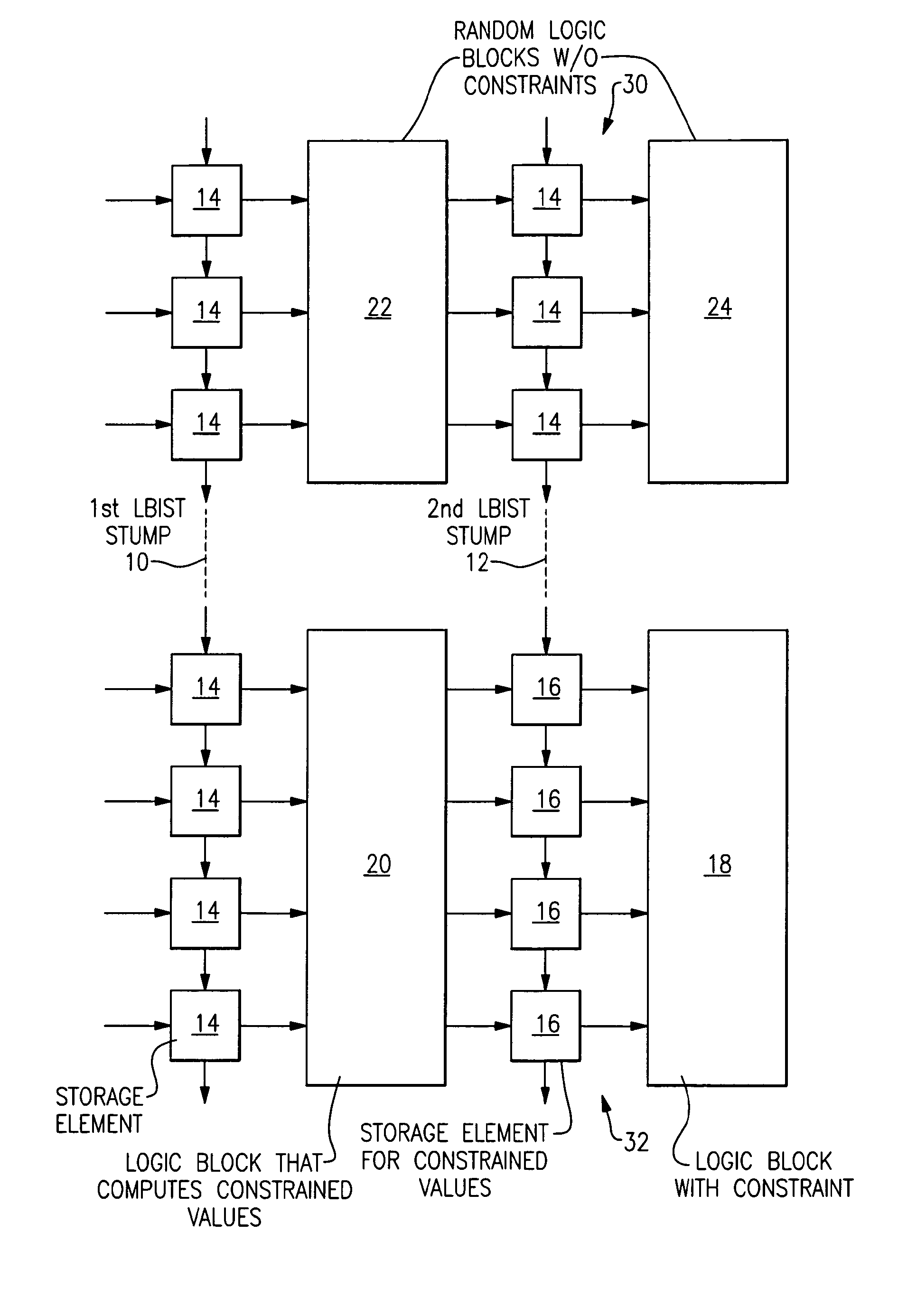
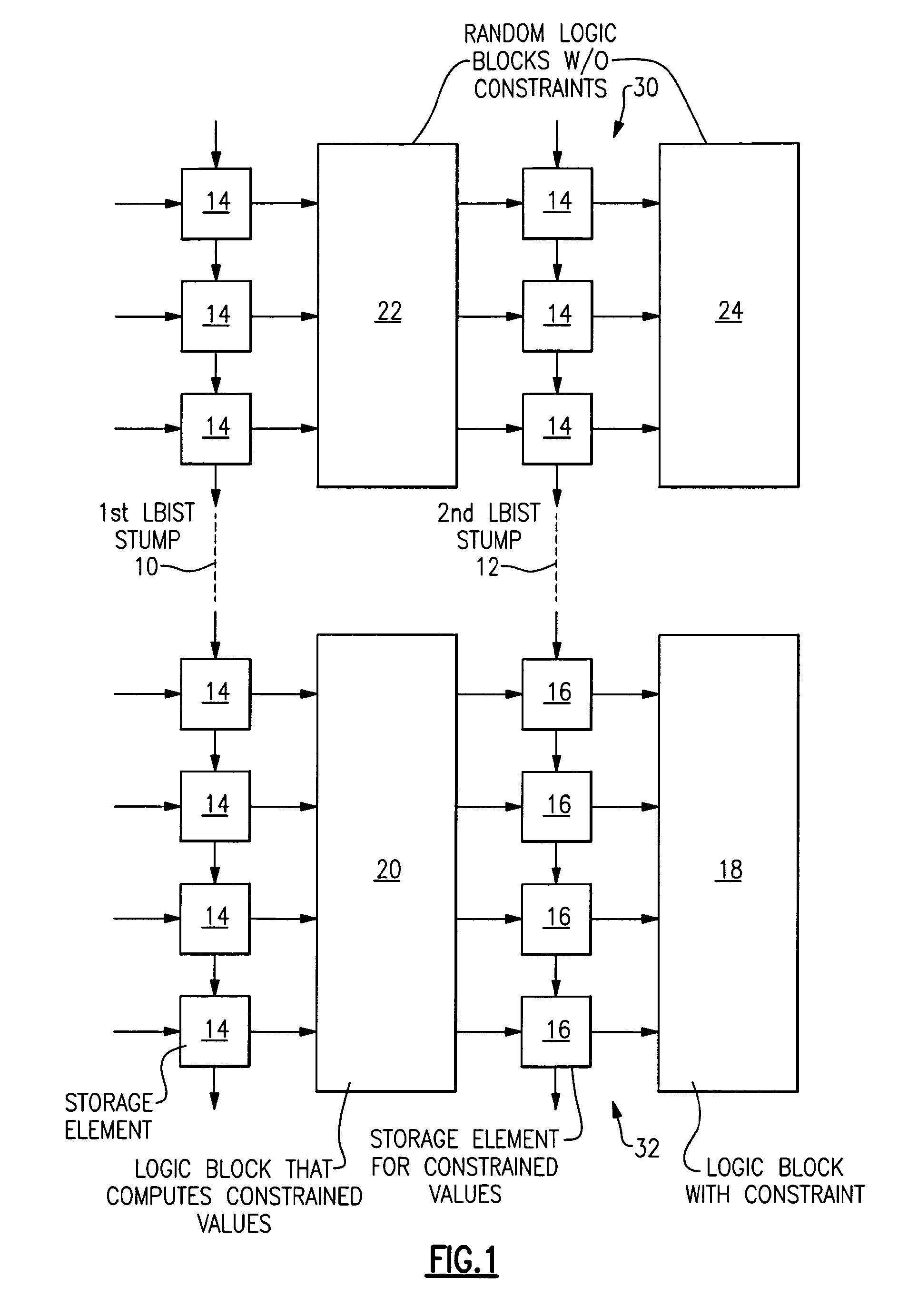
[0029]FIG. 1 illustrates a schematic diagram of a part of an integrated circuit with a logic built-in-self-test (LBIST) engine according to the present invention. The integrated circuit includes a first LBIST stump 10 and a second LBIST stump 12. The first LBIST stump 10 comprises a plurality of storage elements 14 for unconstrained values. The second LBIST stump 12 comprises a first portion 30 and a second portion 32. The first portion 30 of the second LBIST stump 12 includes a plurality of storage elements 14 for unconstrained values. The second portion 32 of the second LBIST stump 12 includes a plurality of storage elements 16 for constrained values. Thus, the second LBIST stump 12 comprises storage elements 14 for unconstrained values as well as storage elements 16 for constrained values. The first LBIST stump 10 comprises only storage elements 14 for unconstrained values in this embodiment.

[0030]The storage elements 14 and 16 are scan-able storage elements. Each storage element...


PUM


Abstract

The present invention relates to a method for performing a logic built-in self-test (LBIST) on an electronic circuit with a plurality of logic circuits (18, 20, 22, 24) and storage elements (14, 16) connected serially to a number of LBIST stumps (10, 12) between a pseudo-random-pattern generator (26) and a multiple-input-signature register (28), wherein at least one constrained logic circuit (18) requires constrained values as input signals. Said method comprises the following steps: scanning the LBIST stumps (10, 12) with the pseudo-random-pattern generator (26), deactivating the multiple-input-signature register (28), performing a functional update in order to propagate legal values into those storage elements (16), which require constrained values, activating or resetting (51) the multiple-input-signature register (28), and setting or programming a start value in a counter (42) for activating a loop back circuit (34) in order to avoid an overwriting of the well-constrained values in the storage elements (16).

Description

BACKGROUND OF THE INVENTION[0001]1. Field of the Invention[0002]The present invention relates to a method for performing a logic built-in-self-test on electronic circuits, especially on integrated circuits. Further the present invention relates to an electronic circuit with a plurality of storage elements and logic circuits and at least a logic built-in-self-test engine.[0003]2. Description of the Related Art[0004]Integrated semiconductor circuits comprise a plurality of storage elements and logic circuits. The storage elements may be realized as flip-flop elements, for example. The logic circuits may be realized as gate logic circuits. During the manufacturing the integrated circuits have to be tested in order to detect defects on the integrated circuit. An example of such a method is a logic built-in-self-test (LBIST). The logic built-in-self-test allows the test of the chip logic at the clock speed of the system.[0005]The LBIST uses pseudo-random pattern generators (PRPG) to init...

Claims


Application Information

Patent Timeline
Patent Type & Authority Patents(United States)
IPC IPC(8): G01R31/28
CPCG01R31/31716G01R31/31855
Inventor GLOEKLER, TILMANKUGEL, MICHAELLE, THUYENWOEHRLE, MATTHIAS
Owner IBM CORP
Learn More