Nonvolatile semiconductor memory and method for driving the same

a nonvolatile semiconductor and memory technology, applied in semiconductor devices, digital storage, instruments, etc., can solve the problems of difficult to reduce the gate length of the memory cell, unsuitable for enhancing the speed of writing, and inability to read and write data normally, so as to reduce increase the area of the memory cell. , the effect of increasing the resistance of the source diffusion layer

Active Publication Date: 2011-05-10
UNISANTIS ELECTRONICS SINGAPORE PTE LTD +1
View PDF17 Cites 16 Cited by
  • Summary
  • Abstract
  • Description
  • Claims
  • Application Information

AI Technical Summary

Benefits of technology

[0009]Therefore, an object of the present invention is to provide a NOR-type nonvolatile semiconductor memory that can inject electric charge into a charge accumulation layer through the use of an FN tunnel current without compromising large scale integration of memory cells.
[0024]According to this invention, a bit line and a source line can be disposed in such a way that they are laid one on top of another when a nonvolatile semiconductor memory cell is viewed from above, making it possible to form them so as to become parallel to each other without increasing the area of the memory cell. When high voltage is applied to a gate line, all the memory cells connected to the gate line are brought into conduction. As a result of the source line being formed so as to be parallel to the bit line, it is possible to apply the same voltage to the bit line and the source line. That is, it is possible to perform, for a selected one memory cell, injection of electric charge into the charge accumulation layer through the use of the FN tunnel current. Since the source line is formed as a diffusion layer, the resistance thereof becomes high. Therefore, by disposing one transistor at intervals of a predetermined number of (for example, 64) memory cells connected to the bit line and the source line, and connecting the source line to the common source line via the transistor, it is possible to lower the resistance of the source diffusion layer and therefore achieve high-speed reading.

Problems solved by technology

As a result, the current required for writing is of the order of 100 μA per cell, making it unsuitable for enhancing the speed of writing.
In the NOR-type flash memory, due to the above-described writing method it adopts, the short channel effect causes an increase in a leakage current, making it impossible to read and write data normally, and it has become difficult to reduce the gate length of the memory cell.
However, it is difficult to perform, for a selected one memory cell, injection of electric charge into the charge accumulation layer through the use of the FN tunnel current by using the equivalent circuit of the conventional NOR-type flash memory shown in FIG. 1.

Method used


Image

  • Nonvolatile semiconductor memory and method for driving the same
  • Nonvolatile semiconductor memory and method for driving the same
  • Nonvolatile semiconductor memory and method for driving the same

Examples


examples

[0101]Hereinafter, based on an embodiment shown in the drawings, the invention will be described. It is to be understood that the invention is not limited in any way by this embodiment.

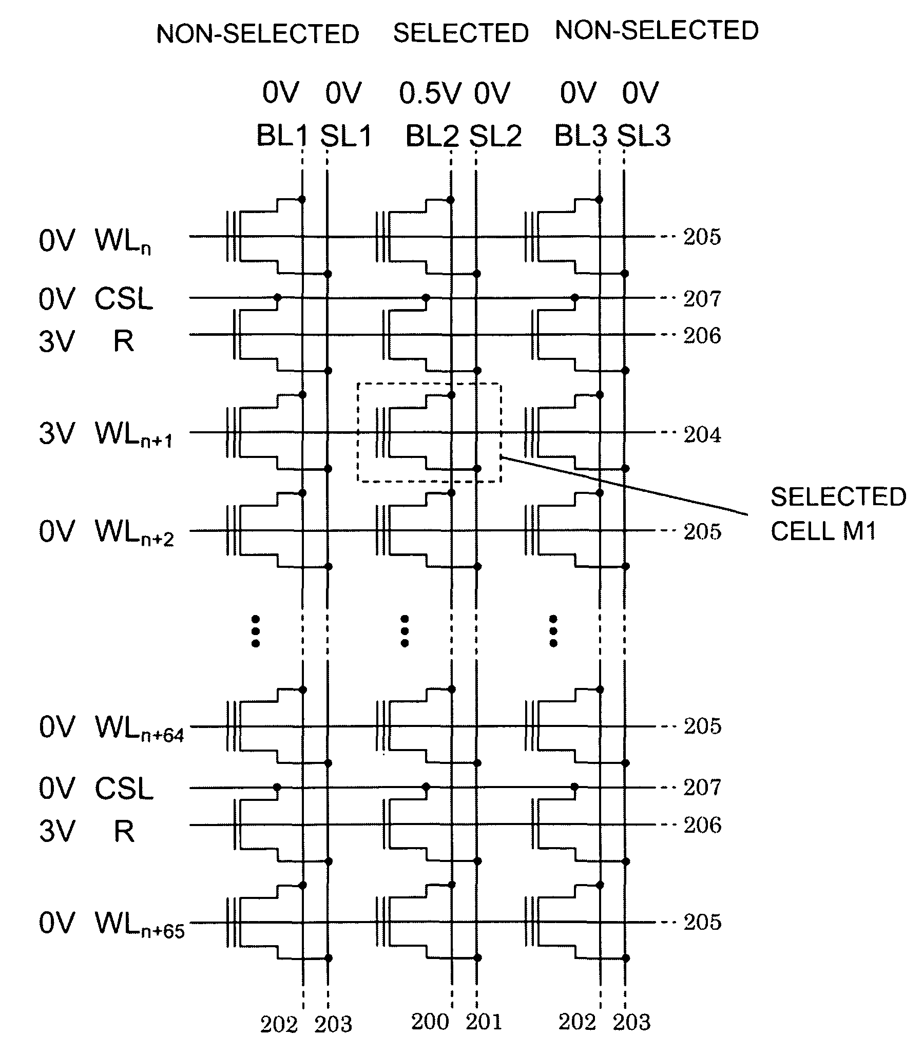
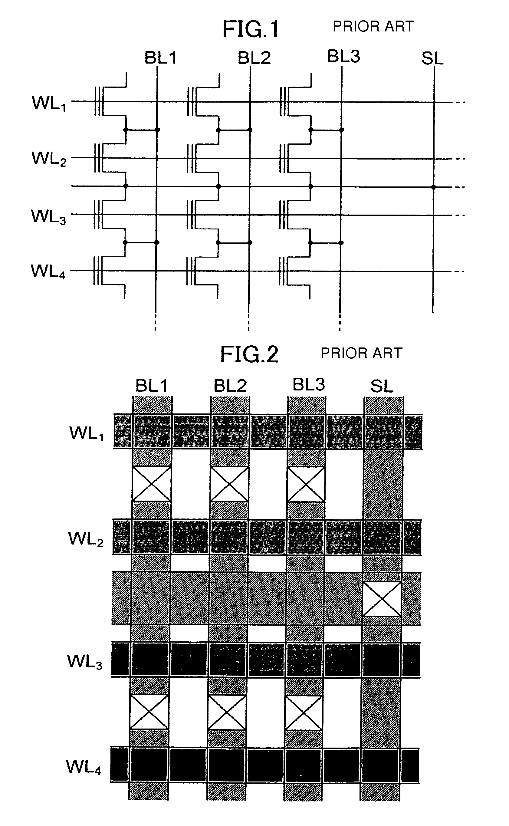
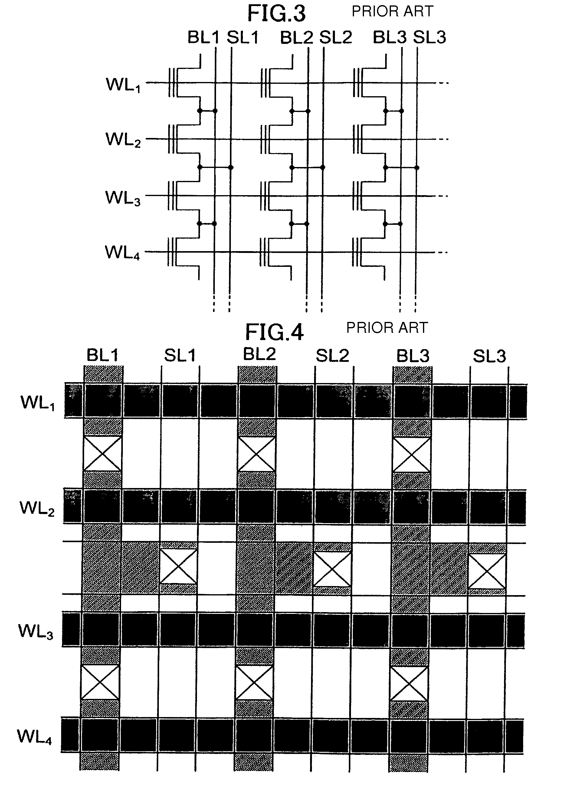
[0102]A layout and a sectional structure of a nonvolatile semiconductor memory according to the invention are shown in FIGS. 5, 6, 7, and 8. In this example, on a silicon oxide film 1, source lines 2 and source diffusion layers 3 are formed, island semiconductor layers 4 are formed thereon, drain diffusion layers 5 are formed in the upper parts of the island semiconductor layers 4, charge accumulation layers 6 formed on the channel regions of the side walls sandwiched between the drain diffusion layers 5 and the source diffusion layers 3 via gate insulation films are formed, and control gates are formed on the charge accumulation layers 6, whereby memory cells are formed. Lines which are laid out in rows so as to connect control gates of memory cells with each other are gate lines 7. In addition, at i...


PUM


Abstract

To provide a NOR-type nonvolatile semiconductor memory that can inject electric charge into a charge accumulation layer through the use of an FN tunnel current without compromising an increase in the packing density of memory cells. The above problem is solved by a nonvolatile semiconductor memory in which nonvolatile semiconductor memory cells are arranged in a matrix, each nonvolatile semiconductor memory cell having an island semiconductor layer in which a drain diffusion layer formed in the upper part of the island semiconductor layer, a source diffusion layer formed in the lower part of the island semiconductor layer, a charge accumulation layer formed on a channel region of the side wall sandwiched between the drain diffusion layer and the source diffusion layer via a gate insulation film, and a control gate formed on the charge accumulation layer are formed. Further, bit lines connected to the drain diffusion layer are laid out in a column direction, control gate lines are laid out in a row direction, and source lines connected to the source diffusion layer are laid out in the column direction.

Description

RELATED APPLICATIONS[0001]This application is a continuation of PCT / JP2007 / 063888, filed on Jul. 12, 2007, which claims priority to Japanese Application No. JP2006-191469, filed on Jul. 12, 2006. The entire contents of these applications are incorporated herein by reference.TECHNICAL FIELD[0002]The present invention relates to a nonvolatile semiconductor memory and a method for driving it.BACKGROUND ART[0003]In a memory cell of a NOR-type flash memory having a control gate and a charge accumulation layer, the one having a MOS transistor structure in which electric charge is injected into the charge accumulation layer through the use of a hot electron has been publicly known (see, for example, T. Tanzawa, Y. Takano, T. Taura, and S. Atsumi, IEEE J. Solid-State Circuits, Vol. 35, no. 10, p. 1415-1421, 2000). Variations in threshold voltage resulting from variations in the charge accumulation state of the charge accumulation layer are stored as data “0”, “1”. For example, in the case o...

Claims


Application Information

Patent Timeline
Patent Type & Authority Patents(United States)
IPC IPC(8): G11C16/04
CPCG11C16/0416H01L27/11521H01L27/11556H01L29/7926H01L29/7881H01L29/792H01L27/11568H10B41/27H10B43/30H10B41/30
Inventor MASUOKA, FUJIONAKAMURA, HIROKI
Owner UNISANTIS ELECTRONICS SINGAPORE PTE LTD
Why Eureka
Try Eureka