

Solid state imaging device having built in signal transfer test circuitry
a solid-state imaging and test circuit technology, applied in the field of data transfer circuits, can solve problems such as difficulty in determining whether the digital value is accurately read, and achieve the effect of accurate reading
- Summary
- Abstract
- Description
- Claims
- Application Information
AI Technical Summary
Benefits of technology
Problems solved by technology
Method used
Image

Examples
Embodiment Construction
[0055]An embodiment of the present invention will be described below, with the embodiment associated with the accompanying drawings.
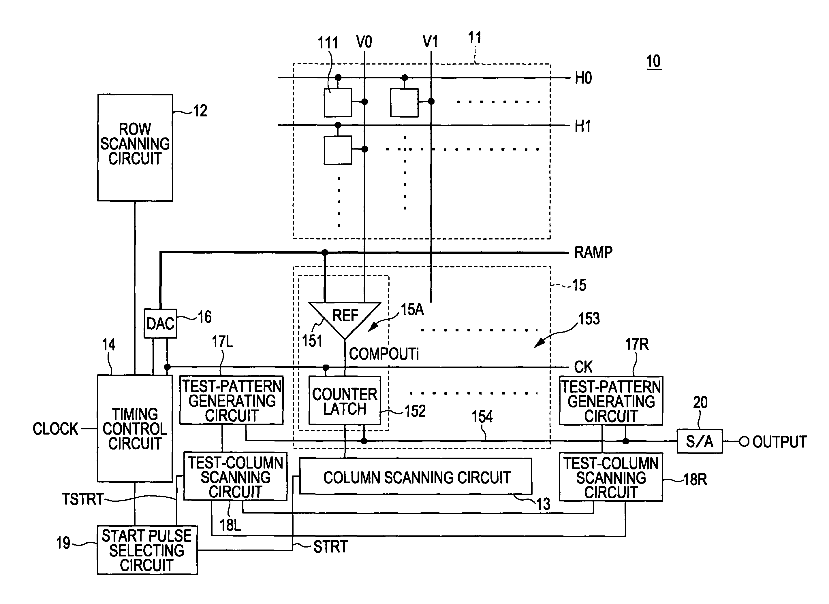
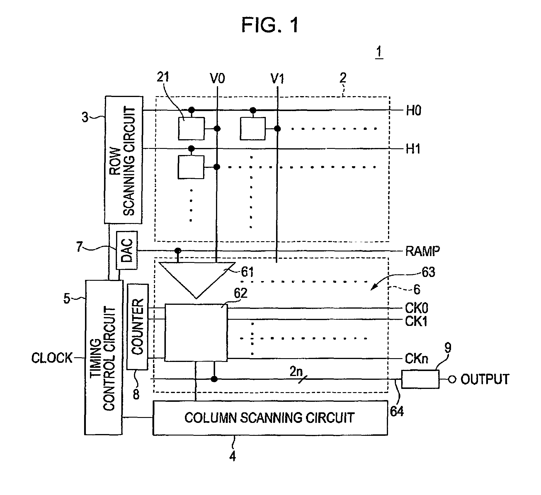
[0056]FIG. 3 is a block diagram showing an example of the configuration of a solid-state imaging device 10 (CMOS image sensor) provided with a column-parallel ADC including a data transfer circuit according to the embodiment of the present invention. FIG. 4 is a block diagram showing more specific configurations of the ADCs shown in FIG. 3 and the solid-state-imaging-device horizontal-transfer and transfer-test systems shown in FIG. 3.
[0057]The solid-state imaging device 10 includes a pixel array section 11 serving as an image pickup section, a row scanning circuit 12, a column scanning circuit 13, a timing control circuit 14, an ADC group 15, a DAC 16, test-pattern generating circuits 17L and 17R, test-column scanning circuits 18L and 18R, a start pulse selecting circuit 19, and a sense amplifier circuit (S / A) 20 serving as a data detecting circuit.
[00...
PUM
 Abstract
Description
Claims
Application Information