Display device

a display device and display terminal technology, applied in the direction of measurement devices, instruments, electrical testing, etc., can solve the problems of difficult alignment of the terminal of the inspection device and the input terminal, and the need for a monitoring facility of the difference current valu

Active Publication Date: 2010-08-03
PANASONIC LIQUID CRYSTAL DISPLAY CO LTD +1
View PDF5 Cites 7 Cited by
  • Summary
  • Abstract
  • Description
  • Claims
  • Application Information

AI Technical Summary

Benefits of technology

[0021]The present invention has been made to overcome the above-mentioned drawbacks of the related art, and it is an advantage of the present invention to provide a technique which, in a display device, can inspect a defect of a photo sensor element and a photo sensor line in response to a turn-on state of a display panel when a predetermined inspection voltage is applied to a photo sensor element via a photo sensor line.
[0022]The above-mentioned and other advantages and novel features of the present invention will become apparent from the description of this specification and attached drawings.
[0023]To briefly explain the summary of typical inventions among inventions disclosed in this specification, they are as follows.
[0024](1) A display device includes a substrate, a plurality of pixels formed on a display region of the substrate, and a plurality of video lines for applying a video voltage to the plurality of pixels, wherein the substrate includes at least one photo sensor element which is formed on a region outside the display region, a photo sensor line which is connected with at least one photo sensor element, and at least one first switching element which connects at least one photo sensor element and at least one video line out of the plurality of video lines, wherein at the time of inspecting the photo sensor element, the first switching element is turned on and, at the same time, a predetermined inspection voltage is applied to at least one photo sensor element via the photo sensor line thus applying a signal to the pixel via the first switching element and the video line, and in response to a turn-on state of the pixel at the time of applying the signal to the pixel, a defect of at least one of at least one photo sensor element and the photo sensor line can be detected.
[0025](2) In the constitution (1), the substrate may be include at least one thin film transistor which constitutes at least one photo sensor element, a first inspection terminal, a second inspection terminal, a third inspection terminal, a first inspection control terminal, a first photo sensor line which constitutes the photo sensor line and connects a first electrode of at least one thin film transistor and the first inspection terminal, a second photo sensor line which constitutes the photo sensor line and connects a second electrode of at least one thin film transistor and the second inspection terminal, a third photo sensor line which constitutes the photo sensor line and connects a control electrode of at least one thin film transistor and the third inspection terminal, and a first inspection control line which connects a control electrode of at least one first switching element and the first inspection control terminal, wherein the first electrode of the thin film transistor may be connected to at least one video line via the first switching element, and at the time of inspecting the photo sensor element, the first switching element may be turned on by applying a control voltage which turns on the first switching element to the first inspection control terminal and, at the same time, the predetermined inspection voltage is applied to at least one thin film transistor via the first to third photo sensor lines thus applying the signal to the pixel via the first switching element and the video line, and in response to the turn-on state of the pixel at the time of applying the signal to the pixel, a defect of at least one of at least one thin film transistor and the first to third photo sensor lines can be detected.
[0026](3) In the constitution (2), the display device may include a group of terminals which are formed on a peripheral portion of the substrate, and a flexible printed circuit board which is electrically and mechanically connected to predetermined terminals of the group of terminals, wherein the group of terminals may include a first photo sensor terminal which is arranged at a position different from the first inspection terminal, a second photo sensor terminal which is arranged at a position different from the second inspection terminal, and a third photo sensor terminal which is arranged at a position different from the third inspection terminal, wherein the first photo sensor terminal may be connected to the first electrode of at least one thin film transistor via the first photo sensor line, the second photo sensor terminal may be connected to the second electrode of at least one thin film transistor via the second photo sensor line, and the third photo sensor terminal may be connected to the control electrode of at least one thin film transistor via the third photo sensor line.

Problems solved by technology

However, this inspection method has a drawback that an inspection facility for monitoring the difference current value becomes necessary.
Further, such an inspection method also has a drawback that respective input terminals of the first to third photo sensor lines have areas smaller than an area of an inspection terminal and hence, it is difficult to align the terminal of the inspection device and the input terminal.

Method used


Image

  • Display device
  • Display device
  • Display device

Examples


Embodiment Construction

[0051]Hereinafter, an embodiment of the present invention is explained in detail in conjunction with drawings.

[0052]Here, in all drawings for explaining the embodiment, parts having identical functions are given same symbols and their repeated explanation is omitted.

[0053]In the embodiment explained hereinafter, the explanation is made with respect to an example which applies the present invention to a liquid crystal display device as one example of a display device.

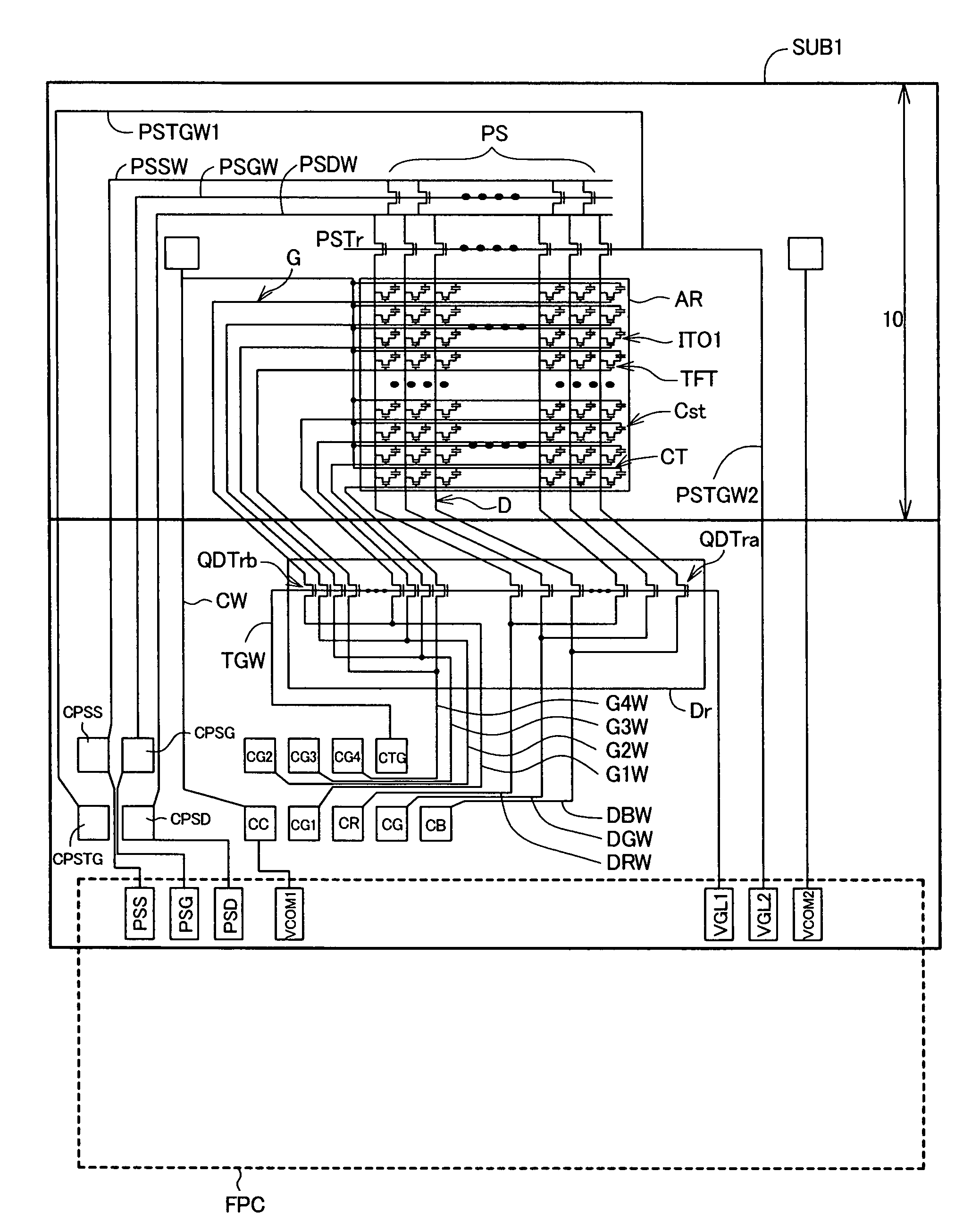
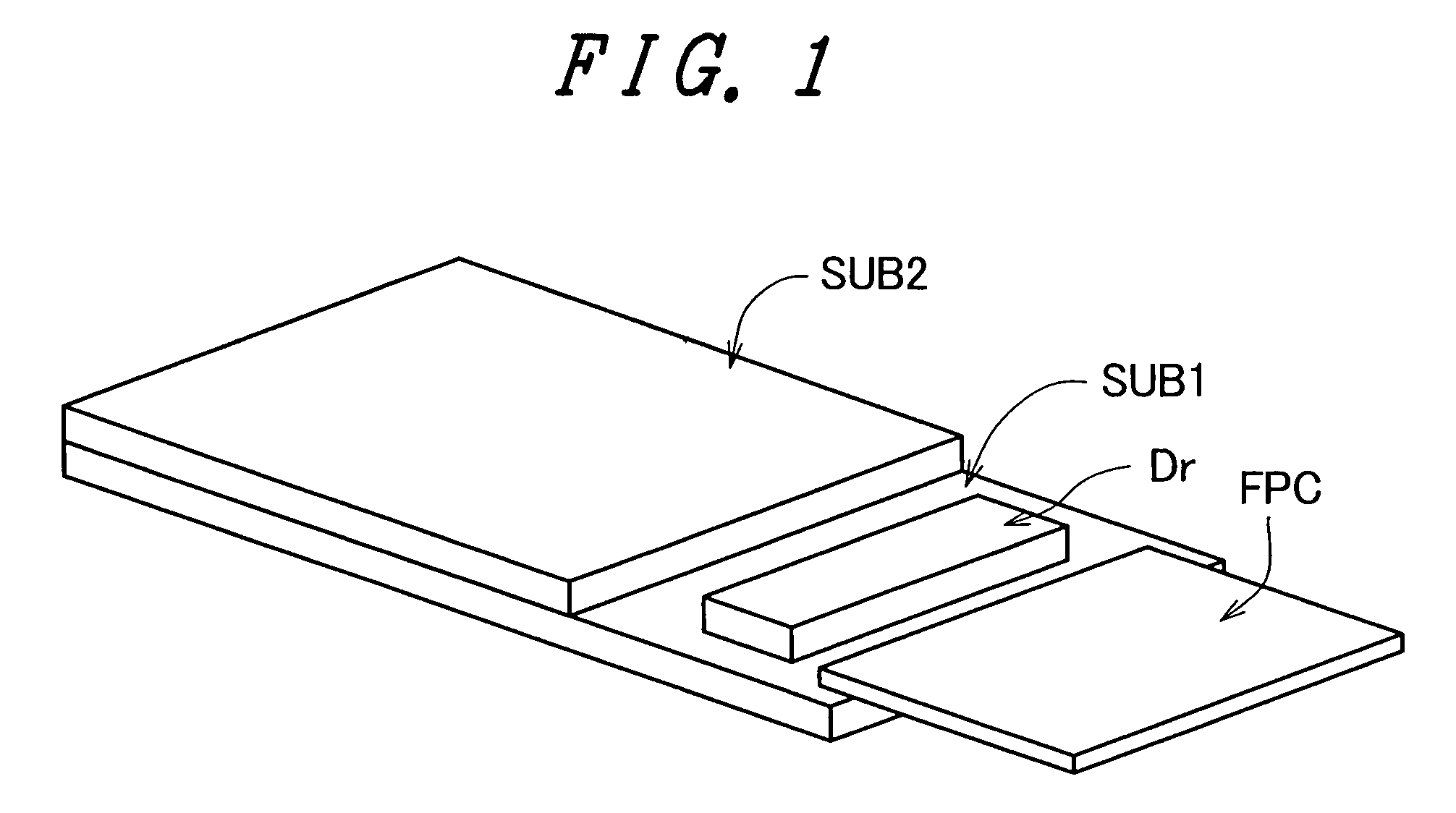
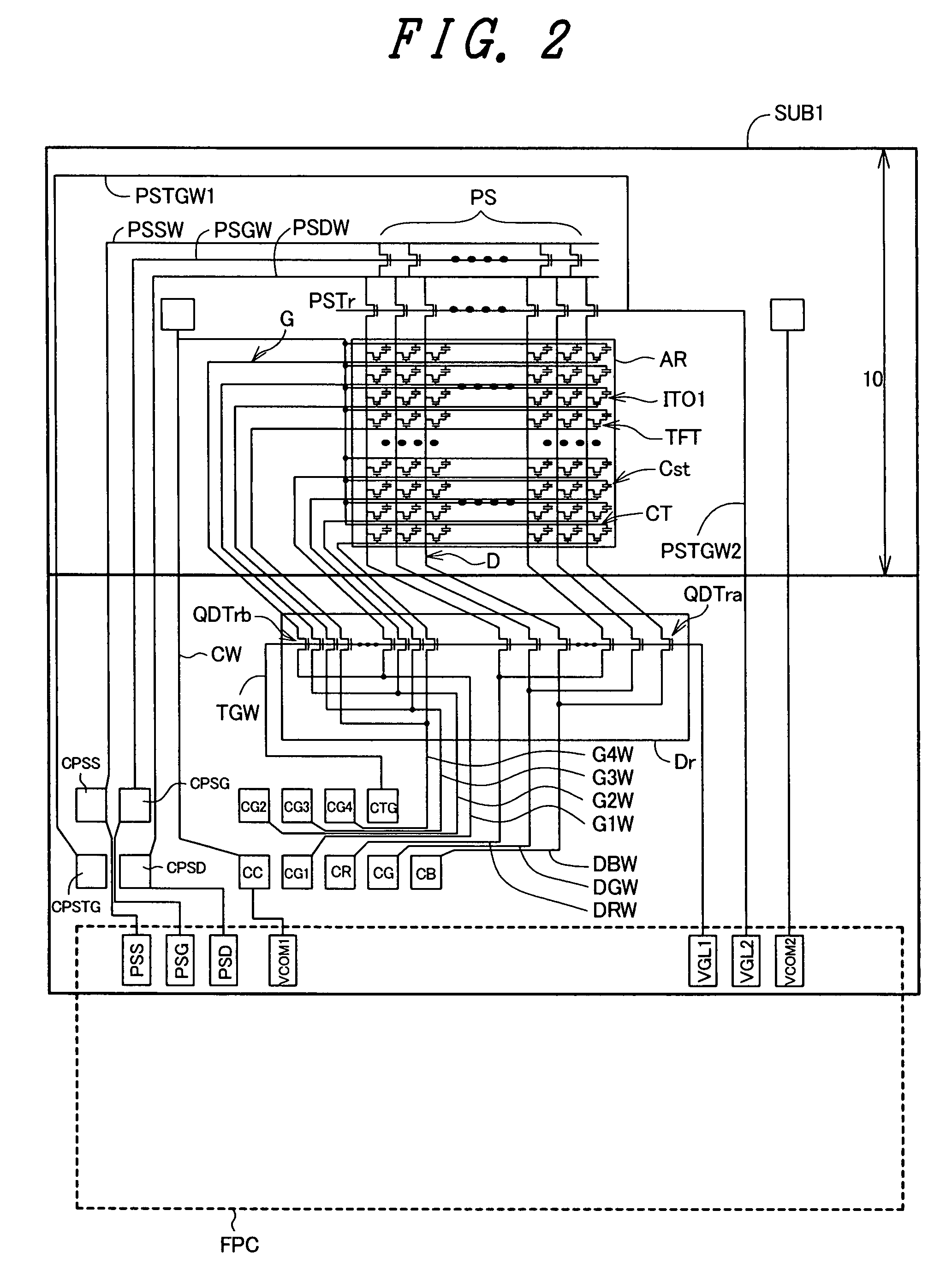
[0054]FIG. 1 is a block diagram showing the schematic constitution of a liquid crystal display panel of a liquid crystal display module of the embodiment according to the present invention. The liquid crystal display module of this embodiment is a miniaturized TFT-type liquid crystal display module which is used as a display part of the mobile phone.

[0055]As shown in FIG. 1. the liquid crystal display panel of this embodiment is configured such that a first substrate (also referred to as a TFT substrate, an active matrix...


PUM


Abstract

The present invention inspects a defect of a photo sensor element or a photo sensor line. A display device includes a substrate, a plurality of pixels formed on a display region of the substrate, and a plurality of video lines for applying a video voltage to the plurality of pixels. The substrate includes at least one photo sensor element which is formed on a region outside the display region, a photo sensor line which is connected with at least one photo sensor element, and at least one first switching element which connects at least one photo sensor element and at least one video line out of the plurality of video lines. At the time of inspecting the photo sensor element, the first switching element is turned on and, at the same time, a predetermined inspection voltage is applied to at least one photo sensor element via the photo sensor line thus applying a signal to the pixel via the first switching element and the video line, and in response to a turn-on state of the pixel at the time of applying the signal to the pixel, a defect of at least one of at least one photo sensor element and the photo sensor line can be detected.

Description

[0001]The present application claims priority from Japanese application JP2006-181249 filed on Jun. 30, 2006, the content of which is hereby incorporated by reference into this application.BACKGROUND OF THE INVENTION[0002]1. Field of the Invention[0003]The present invention relates to a display device, and more particularly to a technique which is effectively applicable to a method for detecting a defect of a display device which includes photo sensor elements within a display panel.[0004]2. Description of Related Art[0005]A TFT-type liquid crystal display module which uses a thin film transistor as an active element can display images of high definition and hence, the TFT-type liquid crystal display module has been used as a display device such as a display for a television receiver set or a personal computer. Particularly, a miniaturized TFT-type liquid crystal display device has been popularly used as a display part of a mobile phone.[0006]In general, with respect to the liquid c...

Claims


Application Information

Patent Timeline
Patent Type & Authority Patents(United States)
IPC IPC(8): G01R31/00
CPCG09G3/006G02F1/13452G09G3/3406G09G2360/145
Inventor YANAGISAWA, SHOISHIGE, NOBUYUKIYAMADA, YASUYUKIITAKURA, HIROKAZU
Owner PANASONIC LIQUID CRYSTAL DISPLAY CO LTD
Why Eureka
Try Eureka