
Direct illumination machine vision technique for processing semiconductor wafers

a machine vision and semiconductor technology, applied in the direction of material analysis using wave/particle radiation, optical radiation measurement, instruments, etc., can solve the problems of adversely affecting the ability to distinguish between the objects of the object, the difficulty of utilizing conventional machine vision systems, and the insufficient contrast of conventional illumination techniques between the wafer and the printing screen, etc., to achieve the effect of being observed and detected quickly

Inactive Publication Date: 2012-05-29
COGNEX CORP
View PDF39 Cites 4 Cited by
  • Summary
  • Abstract
  • Description
  • Claims
  • Application Information

AI Technical Summary

Benefits of technology

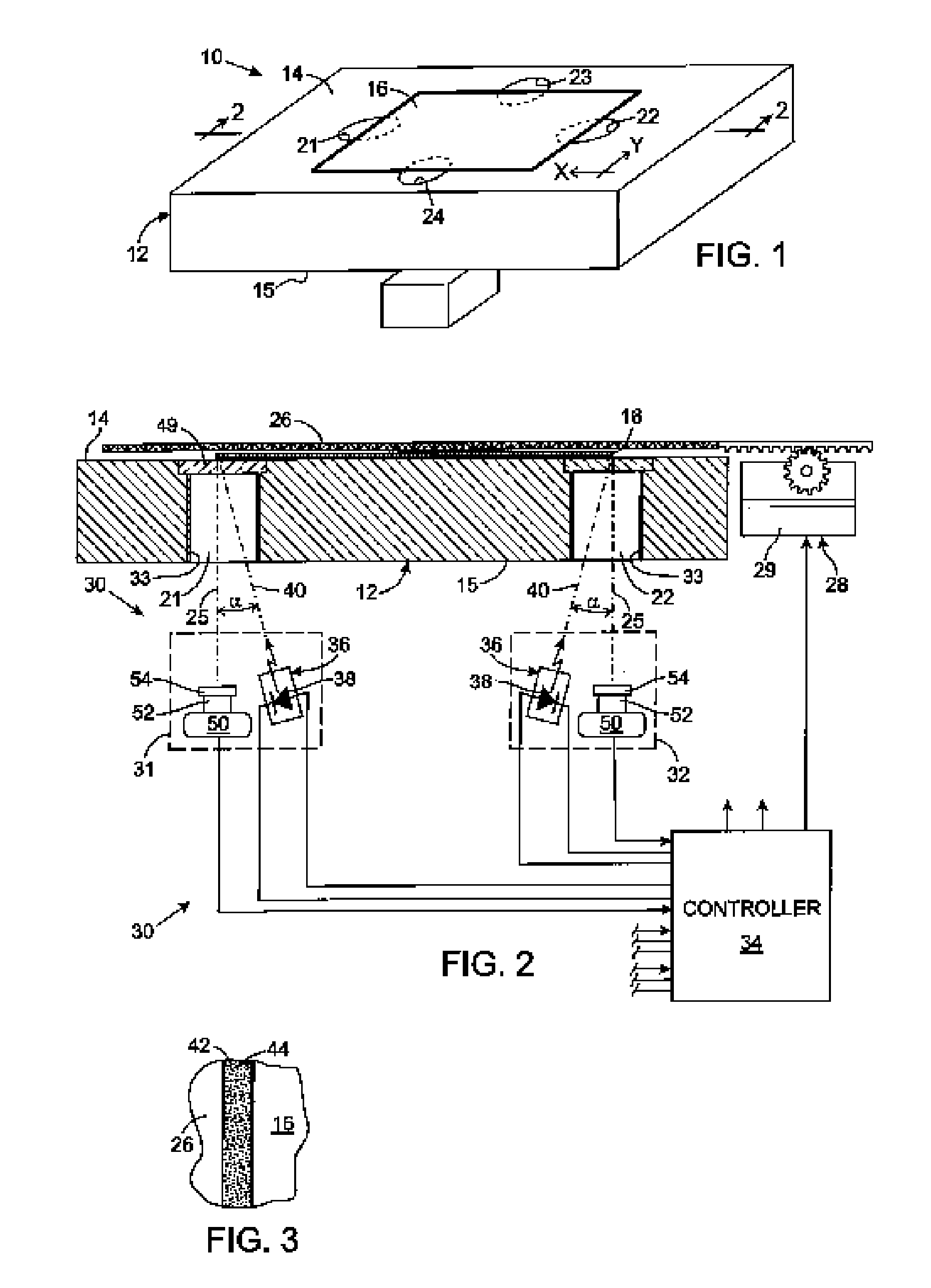
[0011]A video camera, positioned beneath the platen, produces an image using light received from the aperture, wherein some of that light was reflected by the wafer. The relatively dark shadow adjacent the brightly illuminated semiconductor wafer provides a well-defined dark / light transition in the camera image that enables the wafer edge to be readily observed and detected.

Problems solved by technology

Difficulty has been encountered when attempting to utilize conventional machine vision systems to align the printing screen used to deposit the conductive pattern on a photocell wafer.
Conventional illumination techniques did not provide sufficient contrast between the wafer and the printing screen to enable the vision system to reliably and accurately detect the edges of the wafer.
Both the printing screen and the wafer reflect visible light similarly, which adversely affected the ability to distinguish between those objects.
An alternative proposal involved backlighting the printing screen, however placing a light source on the remote side of the printing screen from the wafer interfered with the printing process.

Method used


Image

  • Direct illumination machine vision technique for processing semiconductor wafers
  • Direct illumination machine vision technique for processing semiconductor wafers

Examples


Embodiment Construction

[0016]Although the present invention has particular application for use with equipment for processing photovoltaic device wafers, the vision system has applicability for use in fabricating other types of semiconductor wafers and devices. Furthermore, while the present vision system is being described in the context of an apparatus for printing conductive material on a semiconductor wafer, it can be employed with other kinds of equipment.

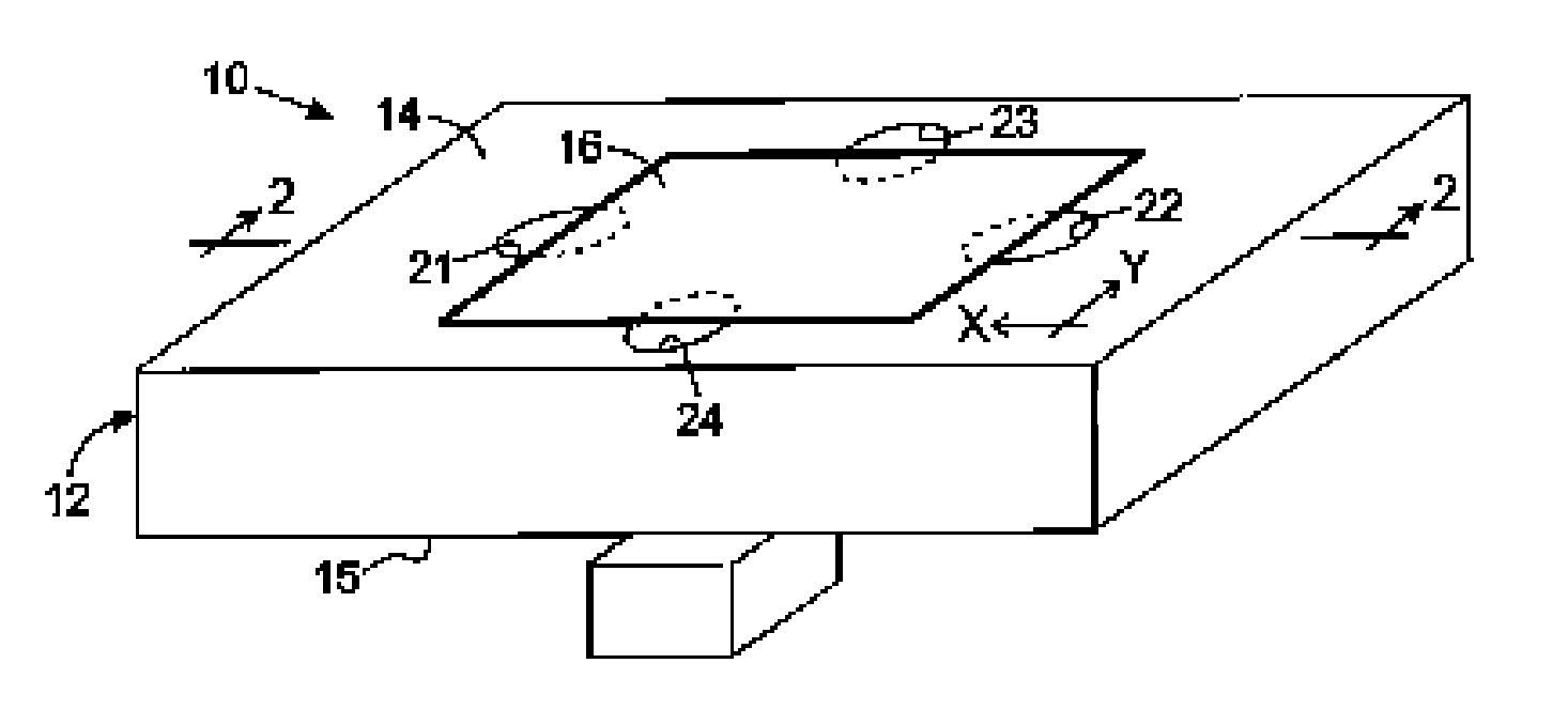
[0017]With initial reference to FIG. 1, an apparatus 10 is employed to apply a conductive pattern of silver to a wafer on semiconductive material in which a photovoltaic device is being fabricated. The apparatus 10 has a platen 12 with a top surface 14 on which the semiconductor wafer 16 is positioned. The exemplary wafer 16 is rectangular, although the present technique can be used with wafers of other shapes by modifying the machine vision system to accommodate such shapes. Four circular viewing apertures 21, 22, 23, and 24 extend through the plate...


PUM


Abstract

A vision system is provided to determine a positional relationship between a semiconductor wafer on a platen and an element on a processing machine, such as a printing screen, on a remote side of the semiconductor wafer from the platen. A source directs ultraviolet light through an aperture in the platen to illuminate the semiconductor wafer and cast a shadow onto the element adjacent an edge of the semiconductor wafer. A video camera produces an image using light received from the platen aperture, wherein some of that received light was reflected by the wafer. The edge of the semiconductor wafer in the image is well defined by a dark / light transition.

Description

CROSS-REFERENCE TO RELATED APPLICATIONS[0001]Not ApplicableSTATEMENT REGARDING FEDERALLY SPONSORED RESEARCH OR DEVELOPMENT[0002]Not ApplicableBACKGROUND OF THE INVENTION[0003]1. Field of the Invention[0004]The present invention relates to processes and equipment for manufacturing semiconductors, such as photovoltaic devices; and more particularly to apparatus and methods for aligning a component of the manufacturing equipment with a wafer of material on which the semiconductors are being fabricated.[0005]2. Description of the Related Art[0006]Semiconductor devices, such as solar cells are fabricated on a wafer of silicon or other material. Various sections of the wafer are electrically interconnected by a pattern of silver or other conductive material deposited on a surface of the wafer. Typically, a screen printing process, similar to silk screen printing element, is employed to deposit the silver in the proper pattern on the wafer surface. The printing screen used in that depositi...

Claims


Application Information

Patent Timeline
Patent Type & Authority Patents(United States)
IPC IPC(8): G01B11/00
CPCG03F9/00G03F9/7065G03F9/7084G03F9/7088
Inventor SCHWAB, JOHN W.LIU, GANGMICHAEL, DAVID J.WANG, LEI
Owner COGNEX CORP
Learn More