Hermetic MEMS device and method for fabricating hermetic MEMS device and package structure of MEMS device

a technology of hermetic mems and device, applied in the manufacture of microstructural devices, semiconductor devices, electrical devices, etc., can solve the problems of high cost, production yield issue, and noise in open environment operation, and achieve the effect of reducing drawbacks

Active Publication Date: 2012-07-10
SOLID STATE SYST
View PDF7 Cites 19 Cited by
  • Summary
  • Abstract
  • Description
  • Claims
  • Application Information

AI Technical Summary

Problems solved by technology

Since the MEMS structure of the MEMS device is sensitive to the environmental air, the operation in open environment may pick up noise.
However, this conventional process has some drawbacks, including high cost, production yield issue due to three elements being packaged into a device, and parasitic effect for the conjunction of MEMS and sensing IC.

Method used


Image

  • Hermetic MEMS device and method for fabricating hermetic MEMS device and package structure of MEMS device
  • Hermetic MEMS device and method for fabricating hermetic MEMS device and package structure of MEMS device
  • Hermetic MEMS device and method for fabricating hermetic MEMS device and package structure of MEMS device

Examples


Embodiment Construction

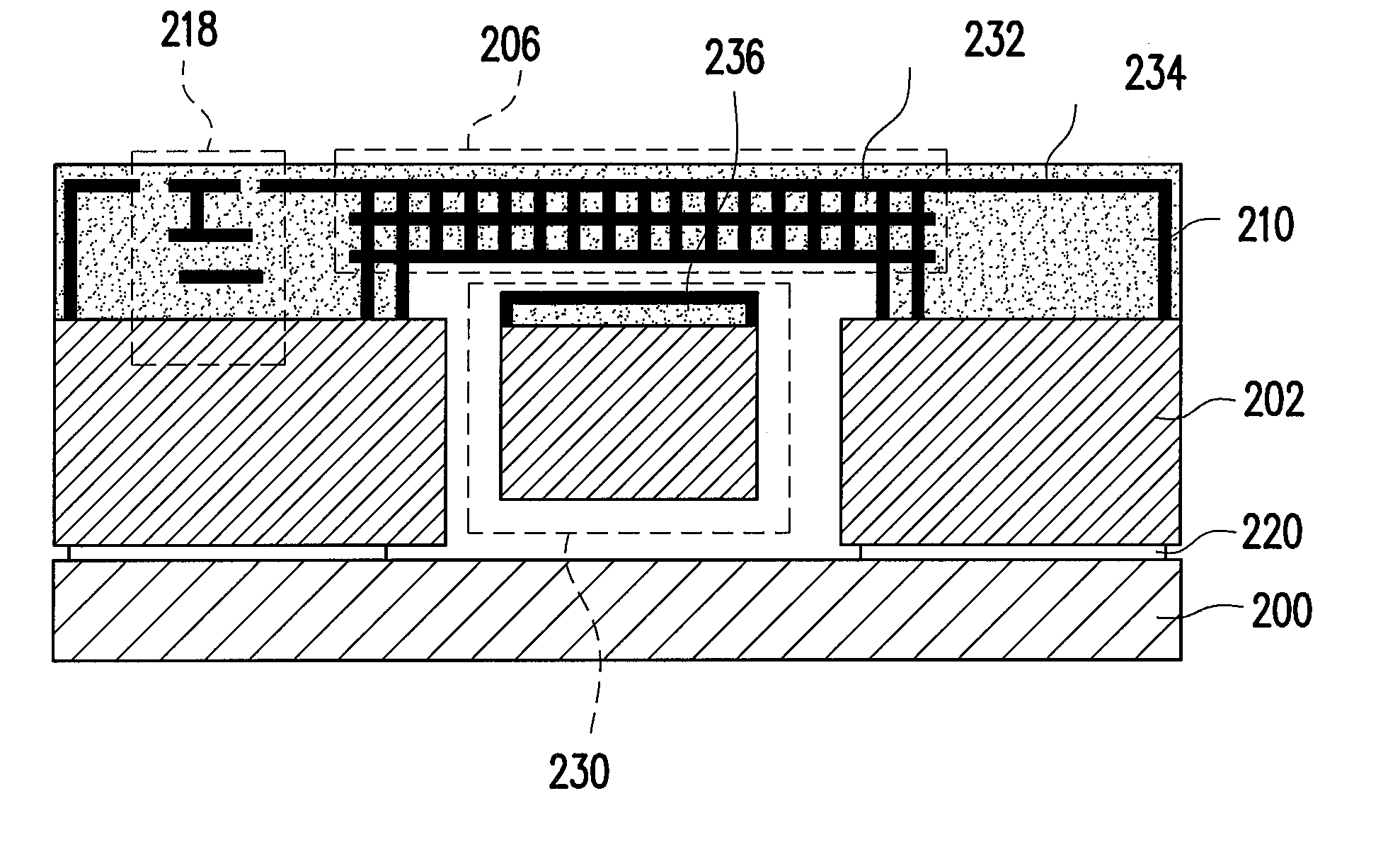
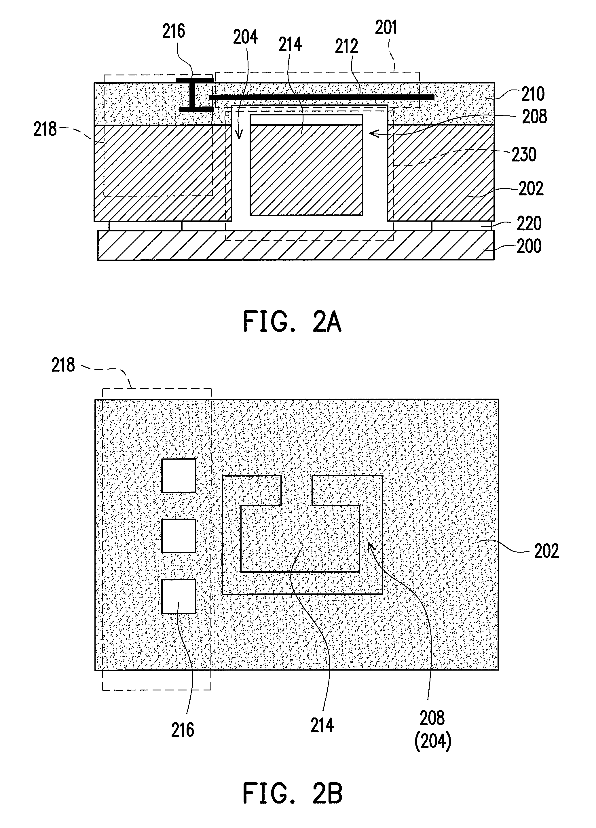
[0041]In the disclosure of the invention, a novel hermetic MEMS device in several embodiments has been proposed. The hermetic MEMS package has at least the following features. The integration between IC and MEMS can increase for high performance. MEMS and sensing IC are manufactures in the same substrate to avoid the parasitic effect for the conjunction of MEMS and sensing IC. The hermetic layer can be formed over the one side of MEMS element by interconnection process of known CMOS technology. Chip scale package (CSP) and wafer level package (WLP) can be used for small size and low cost process. An extra substrate is attached on the other side of MEMS using wafer-wafer bonding or fusion to form a hermetic package.

[0042]Several embodiments are provided from descriptions. However, the invention is not limited to the disclosure of the embodiments. In addition, the embodiments can also be properly combined to each other.

[0043]FIG. 2A is a cross-sectional view, schematically illustratin...


PUM


Abstract

A hermetic microelectromechanical system (MEMS) package includes a CMOS MEMS chip and a second substrate. The CMOS MEMS Chip has a first substrate, a structural dielectric layer, a CMOS circuit and a MEMS structure. The structural dielectric layer is disposed on a first side of the first structural substrate. The structural dielectric layer has an interconnect structure for electrical interconnection and also has a protection structure layer. The first structural substrate has at least a hole. The hole is under the protection structure layer to form at least a chamber. The chamber is exposed to the environment in the second side of the first structural substrate. The chamber also comprises a MEMS structure. The second substrate is adhered to a second side of the first substrate over the chamber to form a hermetic space and the MEMS structure is within the space.

Description

BACKGROUND[0001]1. Field of Invention[0002]The present invention relates to microelectromechanical system (MEMS) device. More particularly, the present invention relates to a structure of MEMS device and the fabrication process.[0003]2. Description of Related Art[0004]MEMS device has been proposed in various applications. However, the MEMS device usually is staying in an open environment. Since the MEMS structure of the MEMS device is sensitive to the environmental air, the operation in open environment may pick up noise. A hermetic package for MEMS device is then proposed.[0005]A hermetic MEMS package has properties including isolating the MEMS structure from the outside environment. For example, the damping of air and thermal noise can be avoided by forming a vacuum environment for MEMS. In addition, hermetic camber can protects the MEMS device from EM interference and produce a small size MEMS device with high performance and low cost for popularity. The applications for the herm...

Claims


Application Information

Patent Timeline
Patent Type & Authority Patents(United States)
IPC IPC(8): H01L27/14
CPCB81C1/00246B81B2207/015B81B2207/07B81B2207/092B81C2203/0714H01L2224/48091H01L2924/1461H01L2224/48247H01L2924/00014H01L2924/00B81B7/0064
Inventor LEE, CHIEN-HSINGHSIEH, TSUNG-MINLIOU, JHYY-CHENG
Owner SOLID STATE SYST
Why Eureka
Try Eureka