Resonator element and resonator
a resonator element and resonator technology, applied in the field of resonator elements, can solve the problems of reducing the area of the resonator element, complex wiring line arrangement, and large area required for the arrangemen
- Summary
- Abstract
- Description
- Claims
- Application Information
AI Technical Summary
Benefits of technology
Problems solved by technology
Method used
Image
Examples
first embodiment
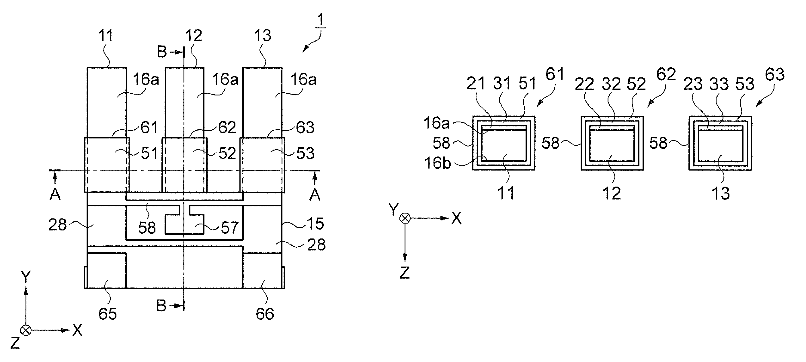
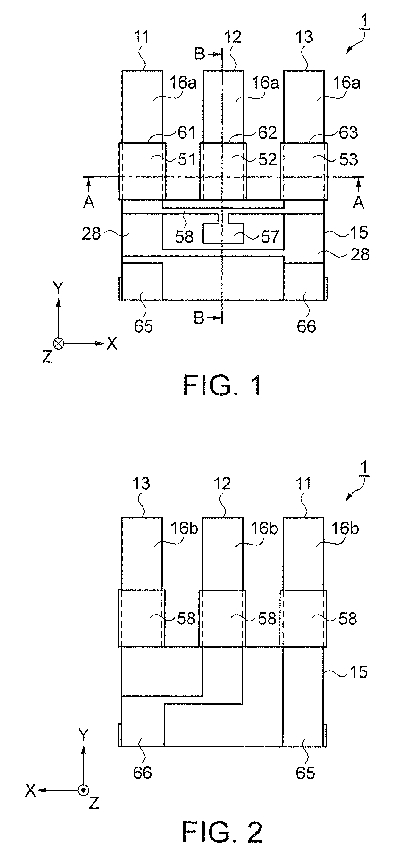
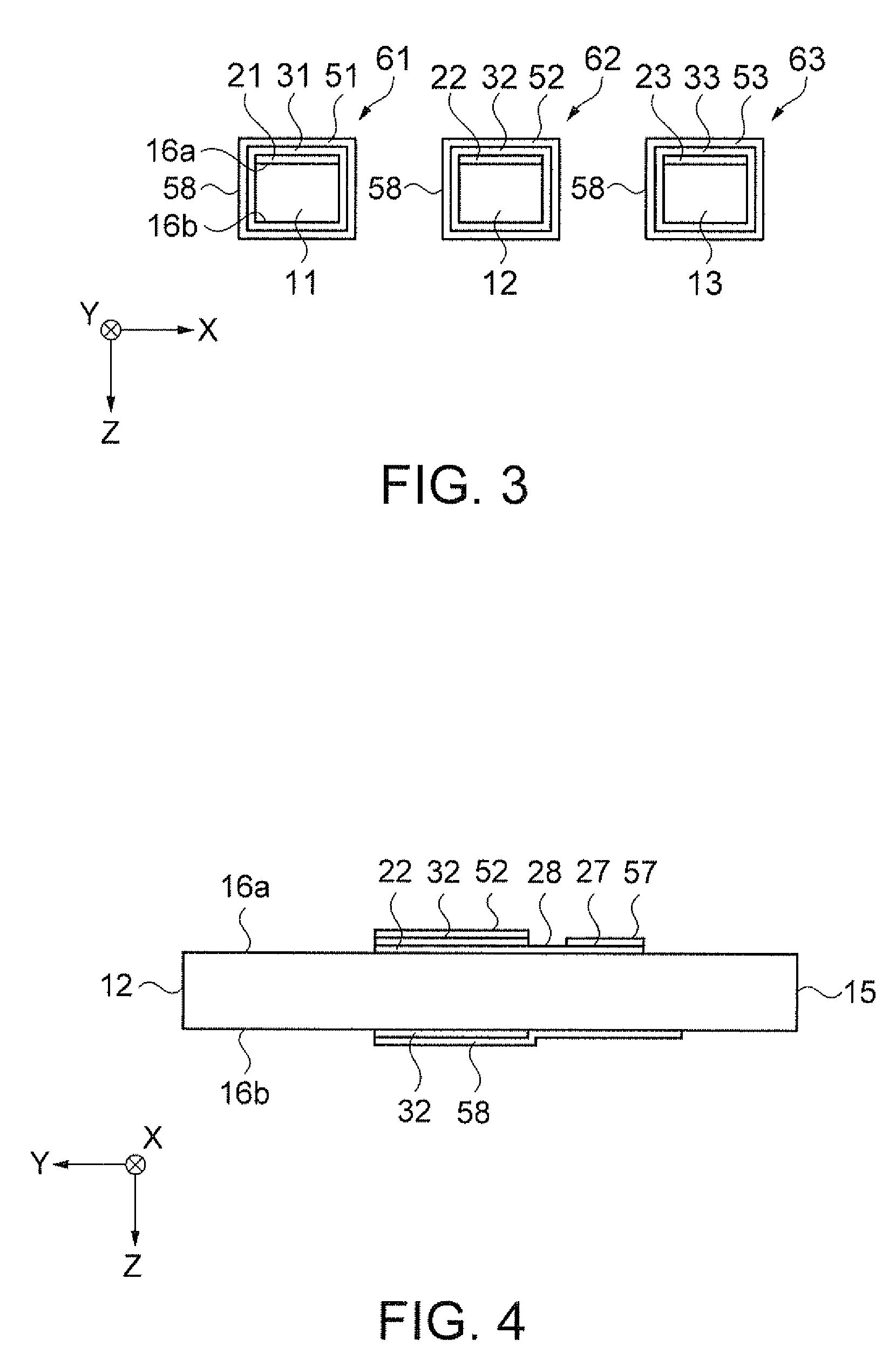
[0041]FIG. 1 is a schematic plan view showing a configuration of a resonator element according to a first embodiment. FIG. 2 is a schematic plan view showing a configuration of a back surface of the resonator element of FIG. 1. FIG. 3 is a schematic sectional view taken along the line A-A of FIG. 1, and shows a configuration of piezoelectric elements. FIG. 4 is a schematic sectional view taken along the line B-B of FIG. 1.
[0042]As shown in FIGS. 1 and 2, a resonator element 1 is formed by employing a base material such as quartz crystal or silicon. The resonator element 1 is in a manner such that a thickness direction thereof is in a Z-direction when the resonator element 1 is developed in an XY-plane in an orthogonal coordinate system. The resonator element 1 has three resonating arms 11, 12, and 13 arranged in an X-direction while extending in parallel with one another in a Y-direction. The resonating arms 11, 12, and 13 are connected to a base 15, so that the resonator element 1 ...
second embodiment
[0077]A resonator element according to a second embodiment will be described. In the present embodiment, an arrangement of wiring lines respectively coupled to the upper electrodes and the lower electrodes is different from that of the first embodiment.
[0078]FIG. 9 is a schematic plan view showing a configuration of a resonator element according to the embodiment. FIG. 10 is a schematic plan view showing a configuration of a back surface of the resonator element of FIG. 9. FIG. 11 is a schematic sectional view taken along the line C-C of FIG. 9, and shows a configuration of piezoelectric elements. FIG. 12 is a schematic sectional view taken along the line D-D of FIG. 9.
[0079]As shown in FIGS. 9 and 10, a resonator element 2 is formed by employing a base material such as quartz crystal or silicon. The resonator element 2 is in a manner such that a thickness direction thereof is in the Z-direction when the resonator element 2 is developed in an XY-plane in an orthogonal coordinate sys...
third embodiment
[0114]As a third embodiment, a resonator equipped with the above-described resonator element will be described.
[0115]FIGS. 16A and 16B show a configuration of the resonator. FIG. 16A is a schematic plan view while FIG. 16B is a schematic sectional view taken along the line G-G of FIG. 16A.
[0116]A resonator 5 includes the resonator element 1, a ceramic package 81 serving as a container, and a lid 85.
[0117]The ceramic package 81 has a recess for housing the resonator element 1. In the recess, a connection pad 88 coupled to the mounting electrodes of the resonator element 1 is provided. The connection pad 88 is coupled to a wiring line in the ceramic package 81, and conductively coupled to an external connection terminal 83 provided to an outer periphery of the ceramic package 81.
[0118]On a periphery of the recess of the ceramic package 81, a seam ring 82 is provided. Further, a through-hole 86 is provided at a bottom of the ceramic package 81.
[0119]The resonator element 1 is bonded an...
PUM
 Abstract
Description
Claims
Application Information


