Three dimensional semiconductor device

a semiconductor device and three-dimensional technology, applied in semiconductor devices, semiconductor/solid-state device details, electrical devices, etc., can solve the problems of difficult large heat generation of semiconductor devices, etc., to facilitate the array and arrangement of semiconductor dies, facilitate the array and placement of semiconductor dies, and facilitate the effect of semiconductor dies

Inactive Publication Date: 2013-04-02
HANA MICRON
View PDF7 Cites 2 Cited by
  • Summary
  • Abstract
  • Description
  • Claims
  • Application Information

AI Technical Summary

Benefits of technology

[0008]Various aspects of the present invention provide a three-dimensional (3D) semiconductor device, which allows a plurality of semiconductor dies to be efficiently arrayed and located, improves heat dissipation efficiency, and facilitates wire bonding and stacking.
[0025]According to exemplary embodiments of the invention, more semiconductor dies can be mounted compared to conventional semiconductor devices. In addition, the semiconductor dies can be easily and efficiently arrayed and arranged.
[0026]Furthermore, a conventional die pad of a lead frame or a substrate is adapted from a fixed shape to facilitate the array and arrangement of semiconductor dies, as well as wire bonding. An area under a semiconductor device is etched, a semiconductor die can be attached onto the etched area, which was not used in the related art, and other semiconductor dies can be attached onto other areas. Accordingly, more semiconductor dies can be efficiently mounted.
[0027]In addition, large portions of the conductive plate are exposed to the outside of the encapsulant, greatly improving heat dissipation efficiency.
[0028]Moreover, symmetrical input and output terminals can be provided on the upper and lower portions, respectively, without compromising the design of the semiconductor device. This, as a result, facilitates stacking in the vertical direction.

Problems solved by technology

However, when a plurality of semiconductor dies is to be attached, it is difficult to array and locate the semiconductor dies.
Furthermore, the semiconductor device generates a great amount of heat as a great number of semiconductor dies are provided.

Method used


Image

  • Three dimensional semiconductor device
  • Three dimensional semiconductor device
  • Three dimensional semiconductor device

Examples


Embodiment Construction

[0054]Reference will now be made in detail to various embodiments of the present invention(s), examples of which are illustrated in the accompanying drawings and described below. While the invention(s) will be described in conjunction with exemplary embodiments, it will be understood that present description is not intended to limit the invention(s) to those exemplary embodiments. On the contrary, the invention(s) is / are intended to cover not only the exemplary embodiments, but also various alternatives, modifications, equivalents and other embodiments, which may be included within the spirit and scope of the invention as defined by the appended claims.

[0055]Above all, reference should be made to the drawings, in which the same reference numerals and signs are used throughout the different drawings to designate the same or similar components.

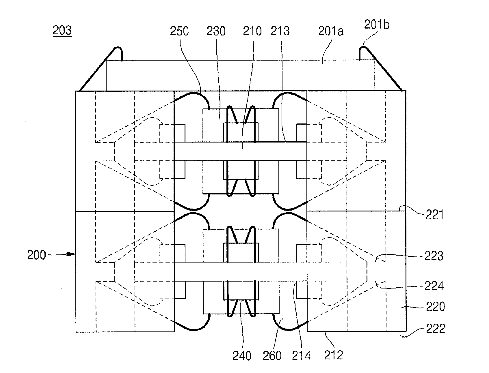
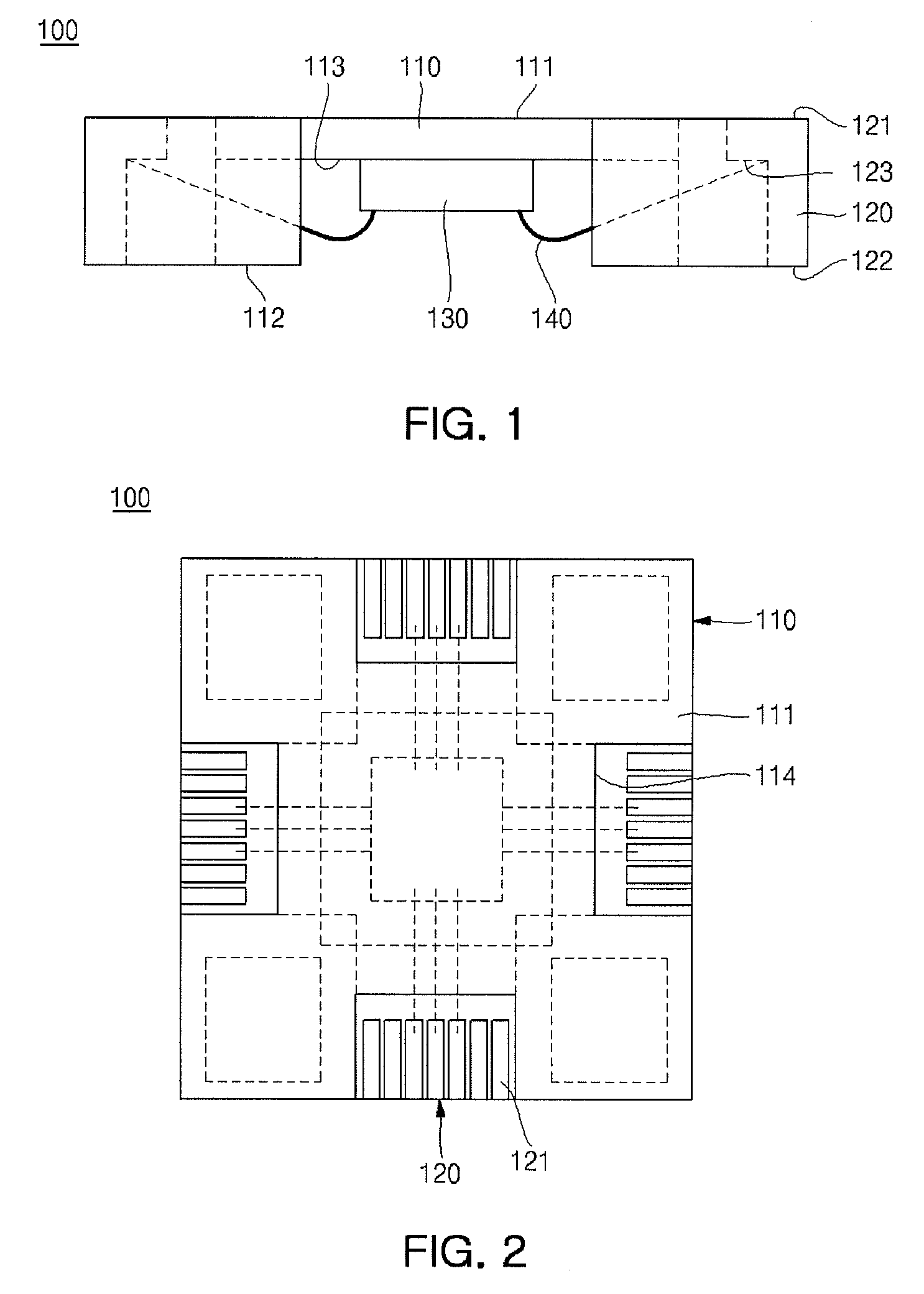
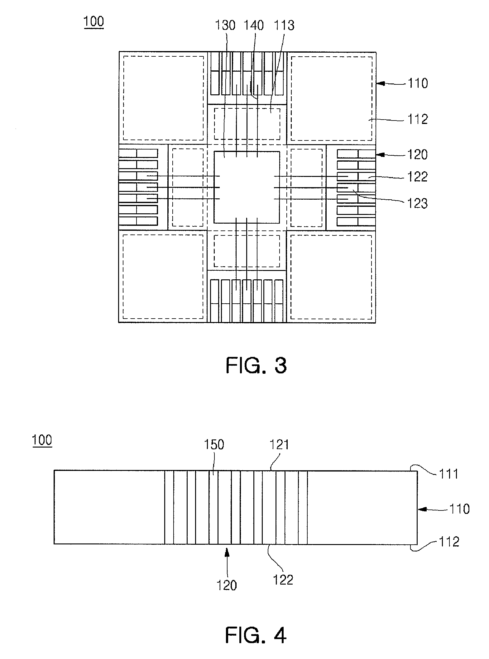
[0056]FIG. 1 is a cross-sectional view illustrating a 3D semiconductor device in accordance with one exemplary embodiment of the invention, aft...


PUM


Abstract

A 3D semiconductor device includes a conductive plate defining four sides and four recesses formed in the four sides, respectively. The conductive plate has first and second surfaces opposite to each other. A plurality of conductive leads are located in the recesses, respectively, and the conductive leads have first and second surfaces opposite to each other. A semiconductor die is attached onto the central area of the conductive plate. A plurality of conductive wires electrically connects the semiconductor die to the conductive leads. An encapsulant encloses, as in a capsule, the conductive plate, the conductive leads, the semiconductor die, and the conductive wires in such a manner that the first and second surfaces of the conductive plate and the first and second surfaces of the conductive leads are exposed to the outside.

Description

CROSS REFERENCE TO RELATED APPLICATION[0001]The present application claims priority to Korean Patent Application Number 10-2008-0127525 filed on Dec. 15, 2008, the entire contents of which application is incorporated herein for all purposes by this reference.BACKGROUND OF THE INVENTION[0002]1. Field of the Invention[0003]The present invention relates to a three-dimensional (3D) semiconductor device.[0004]2. Description of Related Art[0005]As recently electronic appliances have a thin and light profile and support multiple functions, research and development is underway in order to develop semiconductor devices, which can be mounted with a thin profile on electronic appliances while housing a plurality of semiconductor dies.[0006]Most semiconductor devices, and particularly, a semiconductor device including lead frames, have a substantially rectangular die pad onto which a semiconductor die is attached. However, when a plurality of semiconductor dies is to be attached, it is difficul...

Claims


Application Information

Patent Timeline
Patent Type & Authority Patents(United States)
IPC IPC(8): H01L27/06
CPCH01L25/0657H01L2224/48091H01L2224/49175H01L2225/0651H01L2225/0652H01L2225/06541H01L2225/06551H01L2924/01079H01L2924/00014H01L2224/45144H01L2224/45147H01L2924/00H01L2924/01047H01L2224/32145H01L2224/48247H01L23/48H01L23/12
Inventor SHIM, HYUN GUELEE, HEE BONGJEONG, JIN WOOK
Owner HANA MICRON
Why Eureka
Try Eureka