Interconnectable circuit boards

a technology of printed circuit boards and interconnections, which is applied in the direction of semiconductor devices for light sources, coupling device connections, lighting and heating apparatus, etc., can solve the problems of circuit failure, more difficult to reliably solder the connection, and limit and disadvantages of most peopl

Active Publication Date: 2013-08-06
METROSPEC TECH
View PDF140 Cites 24 Cited by
  • Summary
  • Abstract
  • Description
  • Claims
  • Application Information

AI Technical Summary

Problems solved by technology

While there are many types of connections, there are limitations and disadvantages to most of them.
Failure in any one of these joints or reduction in conductivity due to mechanical effects, corrosion or fracture will cause failure of the circuit.
Wires are flexible but are more difficult to reliably solder join and lack the structure for mechanical linkage when this is required.
Flex circuits usually do not add to the mechanical stability or strength of the board-to-board connection.
For almost all of these connection methods described above, protection of the connection from shorting contact, mechanical damage or ESD (electro-static discharge) requires an additional mechanical cover or coating to be added after the solder connection, adding more complexity and cost to the implementation.
Also, most of these interconnection methods present difficulties because of their mechanical sizes, geometries and lack of precise and flat mating surfaces for use on strictly surface mount boards.

Method used


Image

  • Interconnectable circuit boards
  • Interconnectable circuit boards
  • Interconnectable circuit boards

Examples


Embodiment Construction

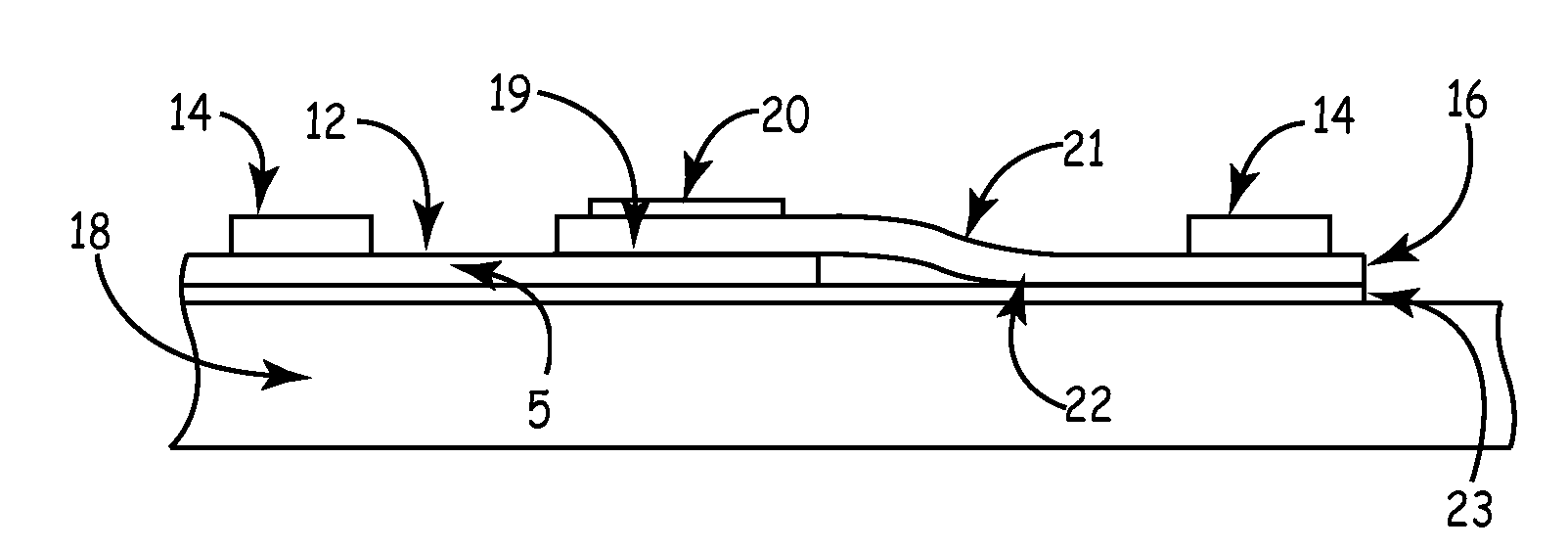
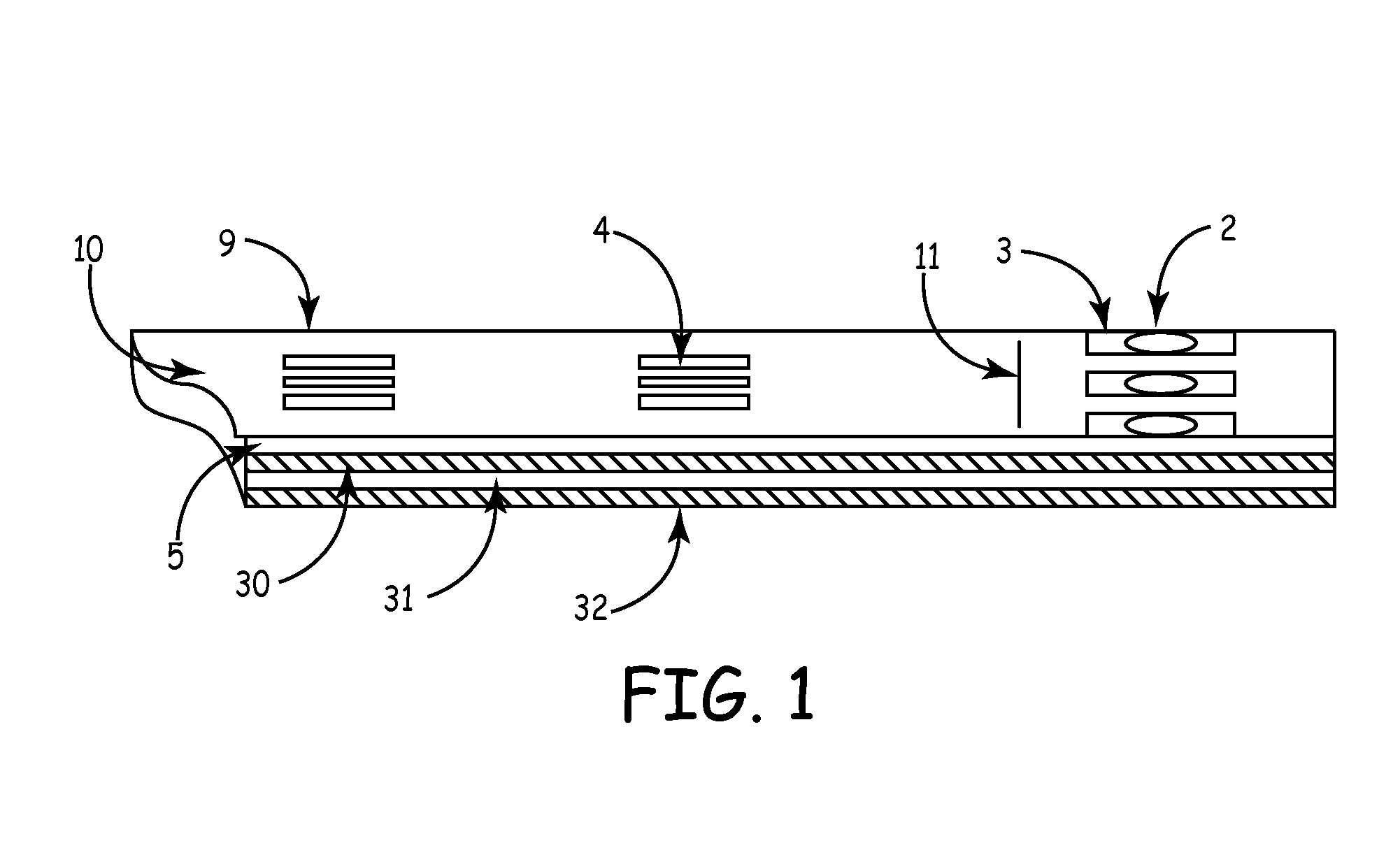
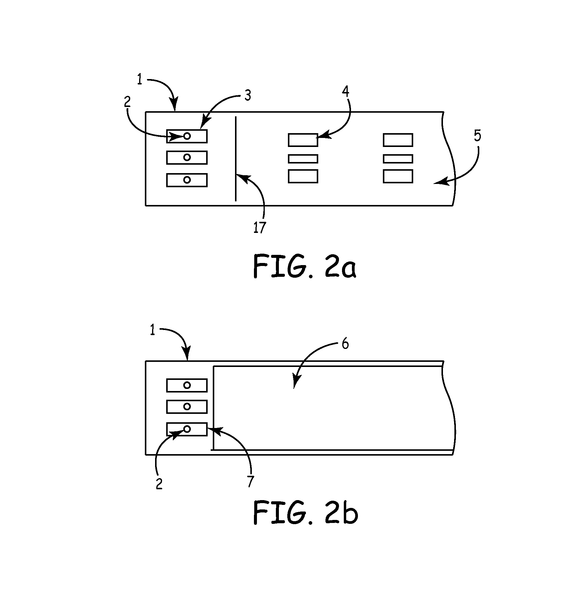
[0035]The following discussion is presented to enable a person skilled in the art to make and use the present teachings. Various modifications to the illustrated embodiments will be readily apparent to those skilled in the art, and the generic principles herein may be applied to other embodiments and applications without departing from the present teachings. Thus, the present teachings are not intended to be limited to embodiments shown, but are to be accorded the widest scope consistent with the principles and features disclosed herein. The following detailed description is to be read with reference to the figures, in which like elements in different figures have like reference numerals. The figures, which are not necessarily to scale, depict selected embodiments and are not intended to limit the scope of the present teachings. Skilled artisans will recognize the examples provided herein have many useful alternatives and fall within the scope of the present teachings.

[0036]The inve...


PUM


Abstract

In some embodiments, an interconnectable circuit board may include one or more of the following features: (a) a first electrically conductive pad located on a top of the circuit board, (b) a plated through hole on the conductive pad which passes through the circuit board, (c) a second electrically conductive pad coupled to the plated through hole; the second conductive pad capable of being electrically connected to a third electrically conductive pad attached to a top of a second interconnectable circuit board, (d) cut marks indicating safe locations for separating the circuit board, and (e) a second cut mark adjacent to the first cut mark where the area between the first and second cut mark can be utilized to make a safe cut through the circuit board.

Description

CROSS-REFERENCE TO RELATED APPLICATIONS[0001]The present application is a continuation application of U.S. patent application Ser. No. 12 / 406,761, filed on Mar. 18, 2009, titled Printed Circuit Board Interconnect Construction, listing Henry V. Holec and Wm. Todd Crandell as co-inventors, herein incorporated by reference in its entirety and claims the benefit of U.S. Patent Application Ser. No. 61 / 037,595, filed on Mar. 18, 2008, titled Front Side Features for Flexible Circuit Boards, listing Henry V. Holec and Wm. Todd Crandell as co-inventors, herein incorporated by reference in its entirety and U.S. Patent Application Ser. No. 61 / 043,006, filed on Apr. 7, 2008, titled Configurations and Controls for High Power LED Systems, listing Henry V. Holec and Wm. Todd Crandell as co-inventors, herein incorporated by reference in its entirety.FIELD OF THE INVENTION[0002]Embodiments of the present invention relate to the design and method of interconnecting printed circuit boards. Particularl...

Claims


Application Information

Patent Timeline
Patent Type & Authority Patents(United States)
IPC IPC(8): H01R12/00
CPCH01R4/02H05K1/14H01R13/717H05K1/118H05K1/0292H05K1/11H01R12/523H05K1/0269H05K1/147H05K3/0061H05K3/363H05K2201/09481H05K2201/09918H05K2201/10106H05K2203/0228F21Y2101/02F21Y2111/005F21Y2115/10F21Y2107/30H01R12/00H05K1/0266H05K1/0293H05K1/0298H05K1/113H05K1/144H05K2201/041H05K2201/2027
Inventor HOLEC, HENRY V.CRANDELL, WM. TODD
Owner METROSPEC TECH
Why Eureka
Try Eureka