

Method for making a light-emitting microelectronic device with semi-conducting nanowires formed on a metal substrate
a technology of semi-conducting nanowires and light-emitting devices, which is applied in the direction of chemically reactive gases, crystal growth processes, polycrystalline materials, etc., can solve the problems of high dislocation rate in the other semi-conducting layers, cumbersome method, and inability to homogeneous current injection on the lower face of the diod
- Summary
- Abstract
- Description
- Claims
- Application Information
AI Technical Summary
Benefits of technology
Problems solved by technology
Method used
Image

Examples
Embodiment Construction
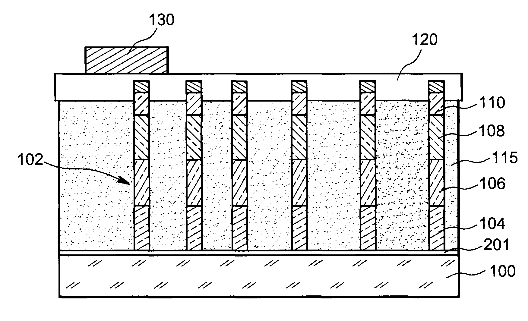
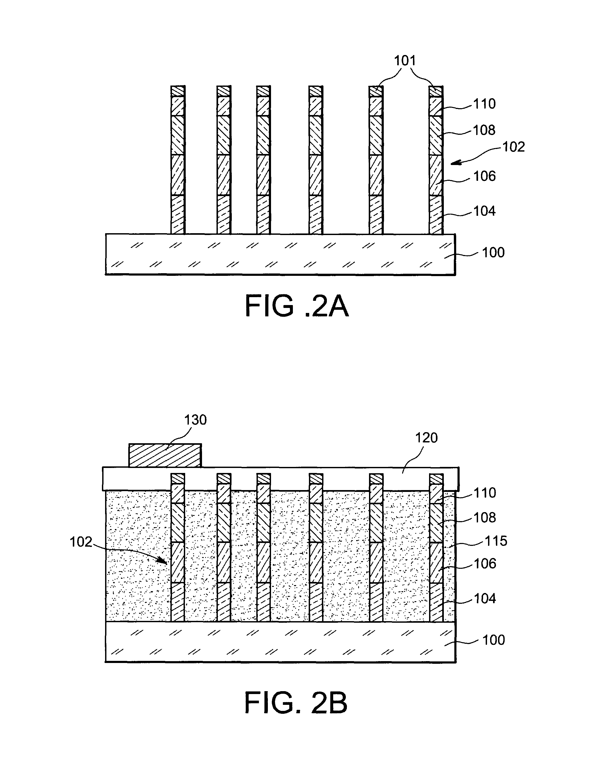
[0028]An exemplary method for making, according to the invention, a light-emitting (LED) microelectronic device, will now be given in connection with FIGS. 2A-2D. The starting material of the method is a substrate 100 which may be based on a metal, for example such as aluminium or silver or copper, or a metal alloy for example based on aluminium or silver or copper, or such as stainless steel or a FeNi alloy, including iron and nickel such as Invar® (registered trade mark by Goodfellow). The metal substrate 100 may have a thickness for example comprised between 10 μm and 10 mm, or for example of the order of 1 mm, and a surface for example comprised between 100 mm2 and 1 m2, or for example of the order of 300 mm2.
[0029]A step for preparing the substrate 100 and in particular a given face of the latter with view to growing wires based on one or several semiconducting materials, may be achieved by means of a surface treatment, for example comprising a step for degreasing the substrate...
PUM
 Abstract
Description
Claims
Application Information