Display device

a display device and double-speed drive technology, applied in semiconductor devices, instruments, electrical apparatus, etc., can solve the problems of insufficient writing, reducing and reducing the writing time by half, so as to suppress waveform distortion, suppress display irregularities, and reduce the transmission coefficient of pixels

Active Publication Date: 2013-10-08
JAPAN DISPLAY INC
View PDF6 Cites 2 Cited by
  • Summary
  • Abstract
  • Description
  • Claims
  • Application Information

AI Technical Summary

Benefits of technology

[0009]An object of the present invention is to provide a display device having pixels disposed in the above-mentioned constitution, which can suppress waveform distortion and lowered transmission coefficient of pixels, and suppress display irregularity.
[0011]According to the present invention, by forming a passivation film with a multilayer structure including an inorganic passivation film, an organic passivation film and an upper inorganic passivation film, and matching the orientations of asymmetrical opening portions in the organic passivation film of pixels adjacent to each other, it is possible to provide a display device which can suppress waveform distortion and lowered transmission coefficient of pixels, and suppress display irregularity.

Problems solved by technology

However, when this constitution is used, it was expected that the following problems occur: since there are two gate signal lines per pixel, the transmission coefficient of pixels is lowered, and writing time is reduced by one half since there is only a single drain signal line and thus the drive frequency is doubled, so that insufficient writing is expected occurs due to the waveform distortion of the drain line.
However, when the above measure was taken in producing a display device, it was found that the problem of display irregularity occurred.

Method used


Image

  • Display device
  • Display device
  • Display device

Examples


first embodiment

[First Embodiment]

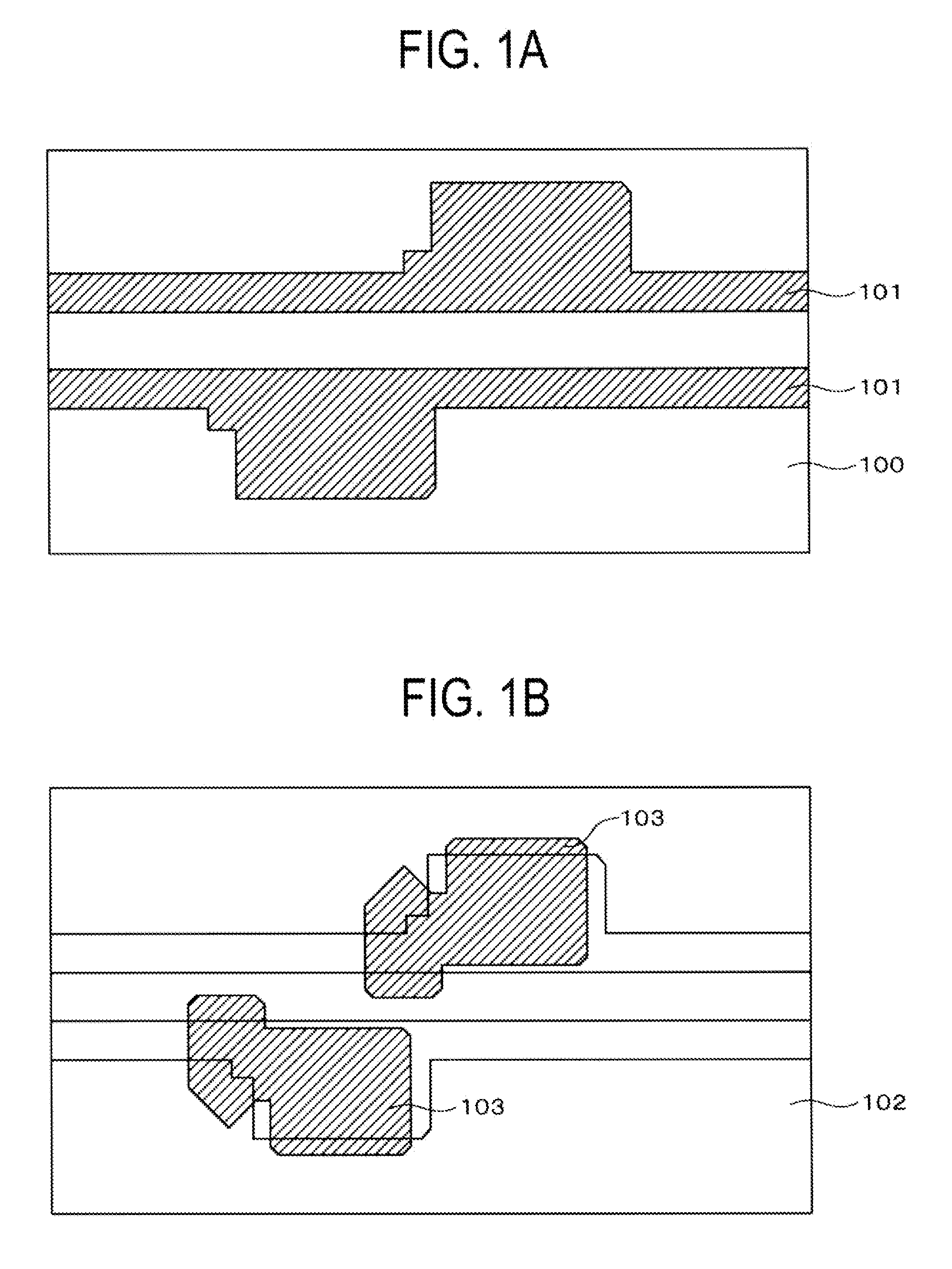
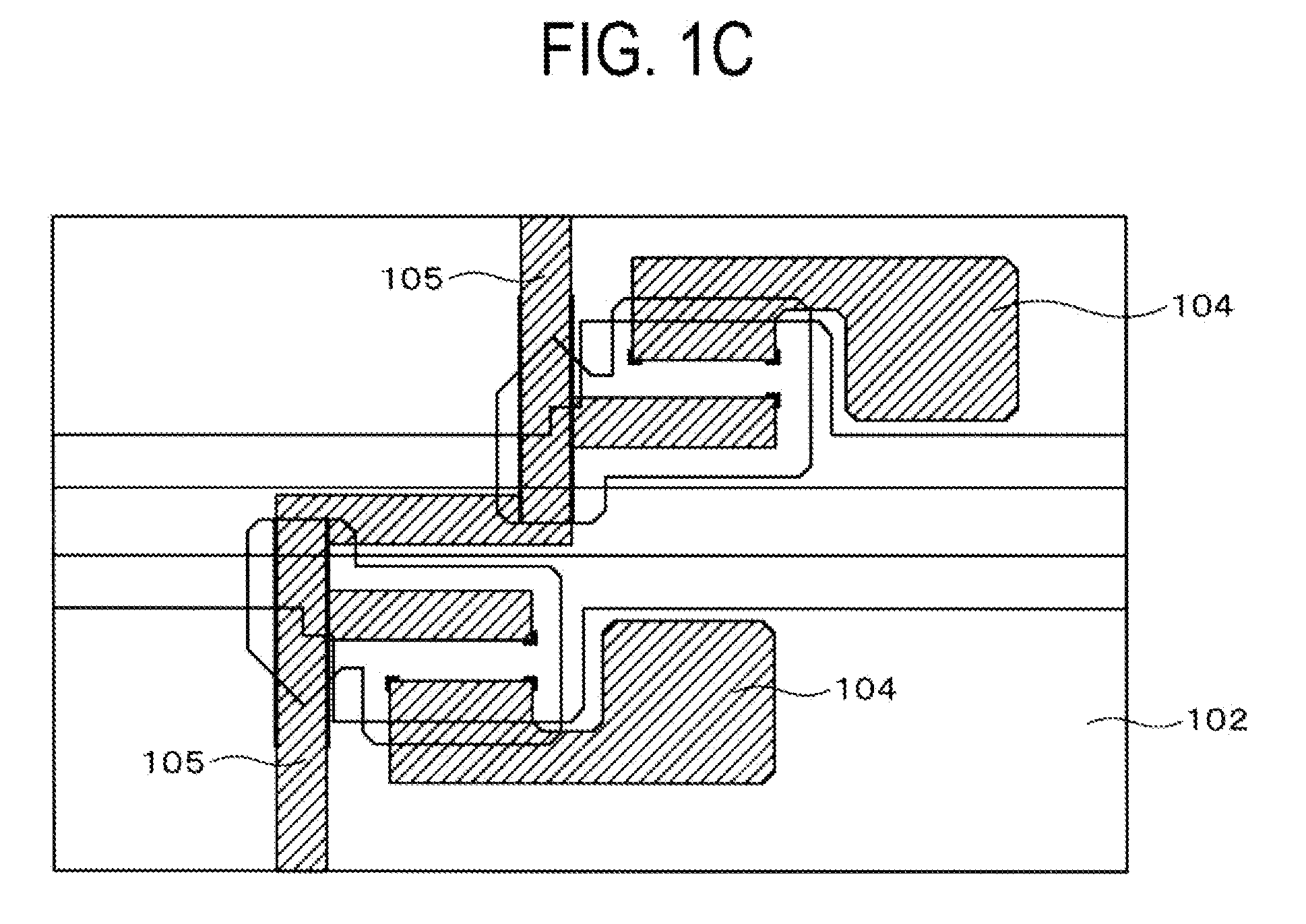
[0032]A first embodiment of the present invention will be described with reference to FIGS. 1A to 1G, 2 and 3.

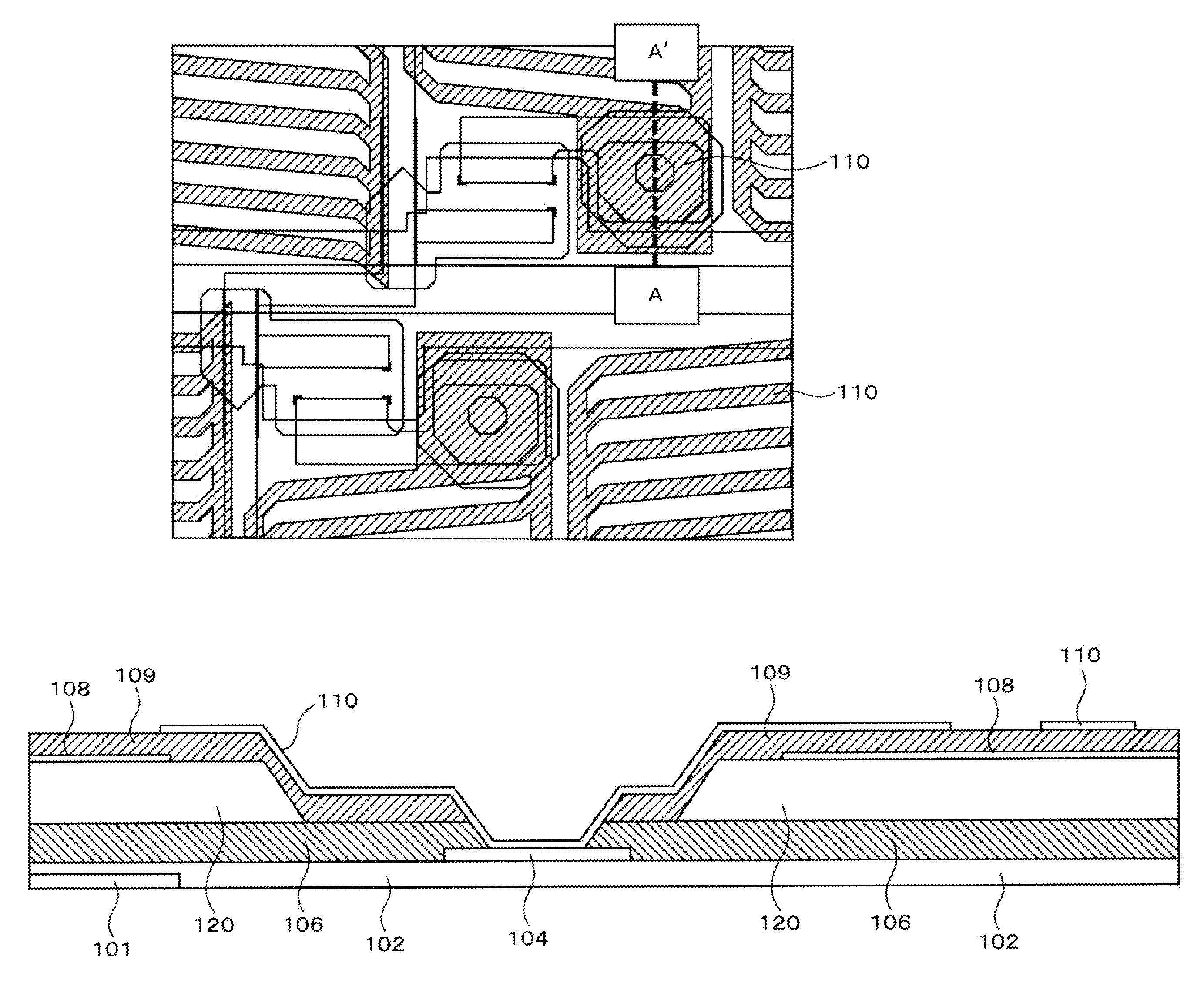
[0033]First, the overall constitution of the liquid crystal display device will be described with reference to FIG. 3. FIG. 3 is a plan view of a liquid crystal display device used for a device such as a cellular phone. In FIG. 3, a counter substrate 200 is placed on a TFT substrate 100. A liquid crystal layer is placed between the TFT substrate 100 and counter substrate 200. The TFT substrate 100 and counter substrate 200 are adhered by a seal 20 formed in a frame portion.

[0034]A portion where no seal is formed on the opposite side of a terminal portion 150 in FIG. 3 becomes a charging hole 21 for liquid crystals, and liquid crystals are charged from this portion. After liquid crystals are charged, the charging hole 21 is sealed by a sealing material 22. The TFT substrate 100 is formed to be larger than the counter substrate 200. In a portion where the TFT...


PUM

PropertyMeasurementUnit
areaaaaaaaaaaa
transmission coefficientaaaaaaaaaa
viewing angleaaaaaaaaaa

Abstract

A display device which can suppress waveform distortion and lowered transmission coefficient of pixels, and suppress display irregularity is provided. In a display device having pixels arranged in a delta arrangement, a pixel includes a pixel portion which comprises a TFT including a source electrode, a drain electrode and a gate electrode, a common electrode and a pixel electrode, an organic passivation film has asymmetrical opening portions above a contact portion of the source electrode, and the orientations of the asymmetrical opening portions in the organic passivation films of pixels adjacent to each other are the same.

Description

CLAIM OF PRIORITY[0001]The present application claims priority from Japanese Patent Application JP 2011-159796 filed on Jul. 21, 2011, the content of which is hereby incorporated by reference into this application.BACKGROUND OF THE INVENTION[0002]1. Field of the Invention[0003]The present invention relates to a double speed drive display device with increased number of scanning lines and reduced number of video signal lines.[0004]2. Description of the Related Art[0005]In a display device, a TFT substrate on which pixels are formed in a matrix pattern having pixel electrodes thin film transistors (TFT) and other components, and a counter substrate opposing the TFT substrate having color filters and other components formed thereon in portions corresponding to those of pixel electrodes of the TFT substrate are disposed. In a liquid crystal display device, liquid crystals are placed between the TFT substrate and counter substrate. An image is formed by controlling the transmission coeff...

Claims


Application Information

Patent Timeline
Patent Type & Authority Patents(United States)
IPC IPC(8): H01L27/14H01L29/15G02F1/1337G02F1/1333H01L31/036H01L29/04
CPCG02F1/136227G02F2001/134372G02F1/134372
Inventor NAGAMI, TAKAHIRO
Owner JAPAN DISPLAY INC
Why Eureka
Try Eureka