Method for fabricating a FinFET device

a technology of finfet and fabrication method, which is applied in the direction of semiconductor devices, basic electric elements, electrical apparatus, etc., can solve the problems of inability to significantly improve the ability to fabricate varied profiles, conventional finfet device fabrication methods are unable to provide varied profiles, and simply changing various process settings

Active Publication Date: 2014-02-18
TAIWAN SEMICON MFG CO LTD
View PDF53 Cites 349 Cited by
  • Summary
  • Abstract
  • Description
  • Claims
  • Application Information

AI Technical Summary

Benefits of technology

[0002]As the semiconductor industry has progressed into nanometer technology process nodes in pursuit of higher device density, higher performance, and lower costs, challenges from both fabrication and design issues have resulted in the development of three dimensional designs, such as a fin-like field effect transistor (FinFET). A typical FinFET is fabricated with a thin “fin” (or fin structure) extending from a substrate, for example, etched into a silicon layer of the substrate. The channel of the FET is formed in this vertical fin. A gate is provided over (e.g., wrapping) the fin. It is beneficial to have a gate on both sides of the channel allowing gate control of the channel from both sides. Further advantages of FinFET devices include reducing the short channel effect and higher current flow.

Problems solved by technology

As the semiconductor industry has progressed into nanometer technology process nodes in pursuit of higher device density, higher performance, and lower costs, challenges from both fabrication and design issues have resulted in the development of three dimensional designs, such as a fin-like field effect transistor (FinFET).
As device structures become more dense, there have been problems associated with fabrication of FinFET devices.
For example, conventional FinFET device fabrication methods are unable to provide varied profiles, such as a square profile, of facets (e.g., Si or SiGe facets) of the fin structure.
Simply changing various process settings has proved incapable of significantly improving the ability to fabricate varied profiles.
The facet profile affects a contact salicidation area, which in conventional FinFET devices may be smaller than desirable, resulting in higher than desirable salicide contact resistance, and thus poor device performance.
Further, in conventional FinFET device fabrication methods, a fin structure height is limited by a fin structure width, for example, because of faceting.
As devices become smaller, the fin structure height limitation further exacerbates the shrinking contact salicidation area issue.

Method used


Image

  • Method for fabricating a FinFET device
  • Method for fabricating a FinFET device
  • Method for fabricating a FinFET device

Examples


Embodiment Construction

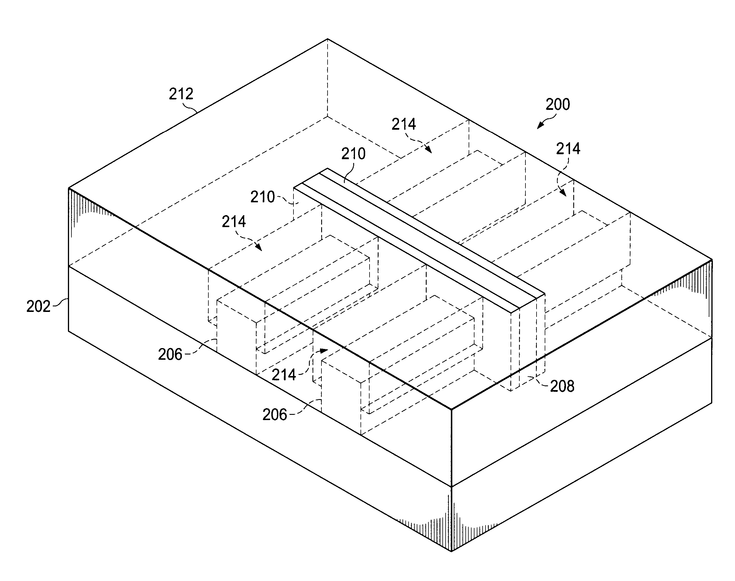
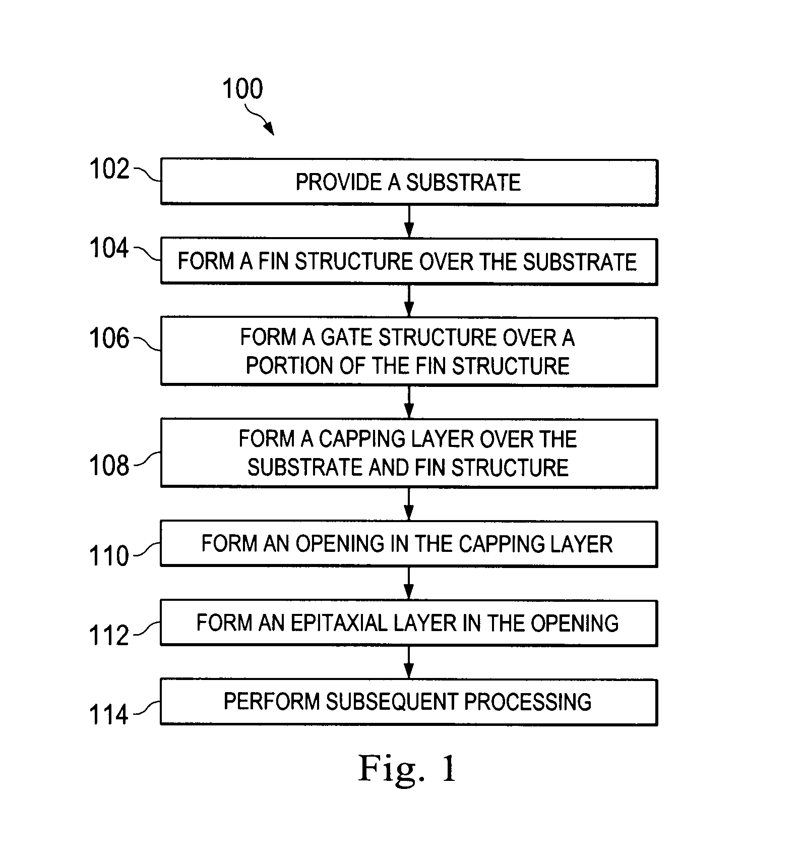
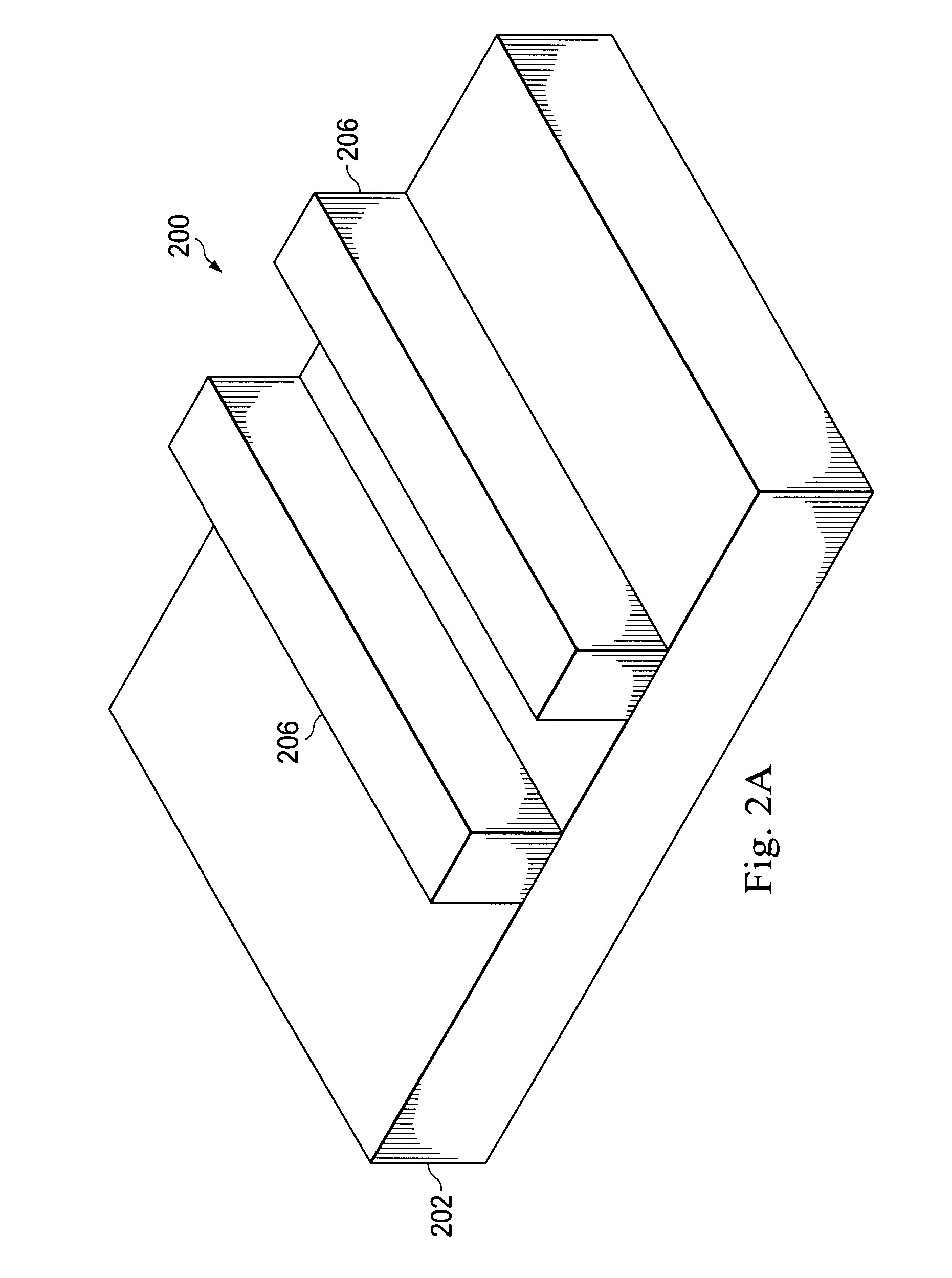
[0013]The present disclosure relates generally to semiconductor devices, and more particularly, to a FinFET device and methods of fabricating a FinFET device (e.g., element or portion of a device / element).

[0014]It is understood that the following disclosure provides many different embodiments, or examples, for implementing different features of the invention. Specific examples of components and arrangements are described below to simplify the present disclosure. These are, of course, merely examples and are not intended to be limiting. For example, the formation of a first feature over or on a second feature in the description that follows may include embodiments in which the first and second features are formed in direct contact, and may also include embodiments in which additional features may be formed between the first and second features, such that the first and second features may not be in direct contact. In addition, the present disclosure may repeat reference numerals and / o...


PUM


Abstract

A FinFET device and method for fabricating a FinFET device is disclosed. An exemplary method includes forming a fin structure on a semiconductor substrate and forming a gate structure on the fin structure. A capping layer is then formed over the semiconductor substrate, fin structure, and gate structure. The capping layer is patterned to form an opening exposing a second portion of the fin structure. An epitaxial layer is grown in the opening and on the second portion of the fin structure. At least one of a source region and a drain region is provided in the epitaxial layer. The method may continue to remove the capping layer.

Description

PRIORITY DATA[0001]This application is a continuation application of Ser. No. 12 / 703,918, filed on Feb. 11, 2010, entitled “Method For Fabricating A Finfet Device,” the entire disclosure of which is incorporated herein by reference.BACKGROUND[0002]As the semiconductor industry has progressed into nanometer technology process nodes in pursuit of higher device density, higher performance, and lower costs, challenges from both fabrication and design issues have resulted in the development of three dimensional designs, such as a fin-like field effect transistor (FinFET). A typical FinFET is fabricated with a thin “fin” (or fin structure) extending from a substrate, for example, etched into a silicon layer of the substrate. The channel of the FET is formed in this vertical fin. A gate is provided over (e.g., wrapping) the fin. It is beneficial to have a gate on both sides of the channel allowing gate control of the channel from both sides. Further advantages of FinFET devices include red...

Claims


Application Information

Patent Timeline
Patent Type & Authority Patents(United States)
IPC IPC(8): H01L21/336
CPCH01L29/66795H01L29/41791H01L2029/7858H01L29/045H01L29/785
Inventor LIN, HSIEN-HSINKWOK, TSZ-MEISU, CHIEN-CHANG
Owner TAIWAN SEMICON MFG CO LTD
Why Eureka
Try Eureka