Dynamic random access memory unit and fabrication method thereof

a memory unit and random access technology, applied in the direction of semiconductor devices, electrical equipment, transistors, etc., can solve the problems of increasing device density, and achieve the effect of increasing device density

Active Publication Date: 2015-07-30
MICRON TECH INC
View PDF5 Cites 10 Cited by
  • Summary
  • Abstract
  • Description
  • Claims
  • Application Information

AI Technical Summary

Benefits of technology

[0006]The embodiment of the instant disclosure provides a dynamic random access memory unit and the fabrication method thereof. The dynamic random access memory unit has a self-aligned trench isolation structure formed in the bottom portion of the trench of the substrate. Such arrangement results in an increase in device density.

Problems solved by technology

Such arrangement results in an increase in device density.

Method used


Image

  • Dynamic random access memory unit and fabrication method thereof
  • Dynamic random access memory unit and fabrication method thereof
  • Dynamic random access memory unit and fabrication method thereof

Examples


Embodiment Construction

[0016]The instant disclosure will be described more specifically with reference to the following embodiments. It is to be noted that the following descriptions of preferred embodiments are provided herein for purpose of illustration and description. It is not intended to be exhaustive or limiting to the precise form disclosed.

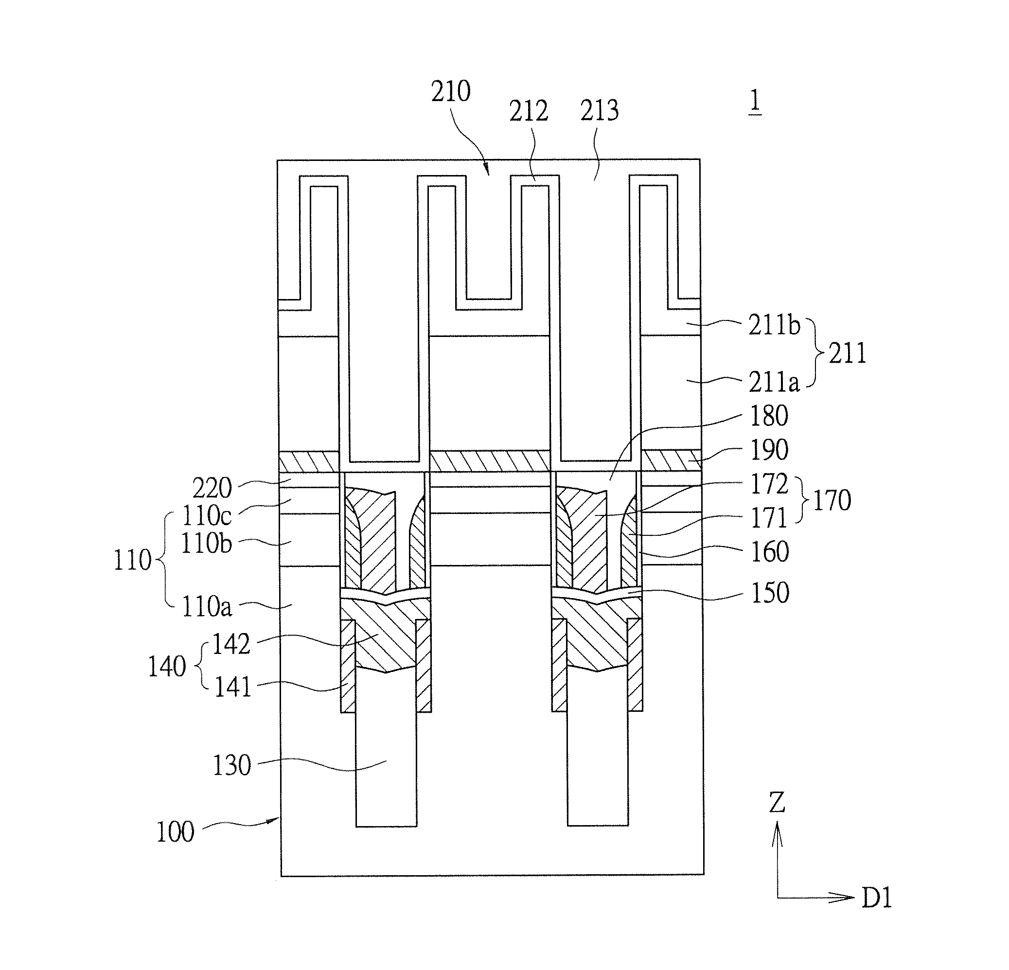
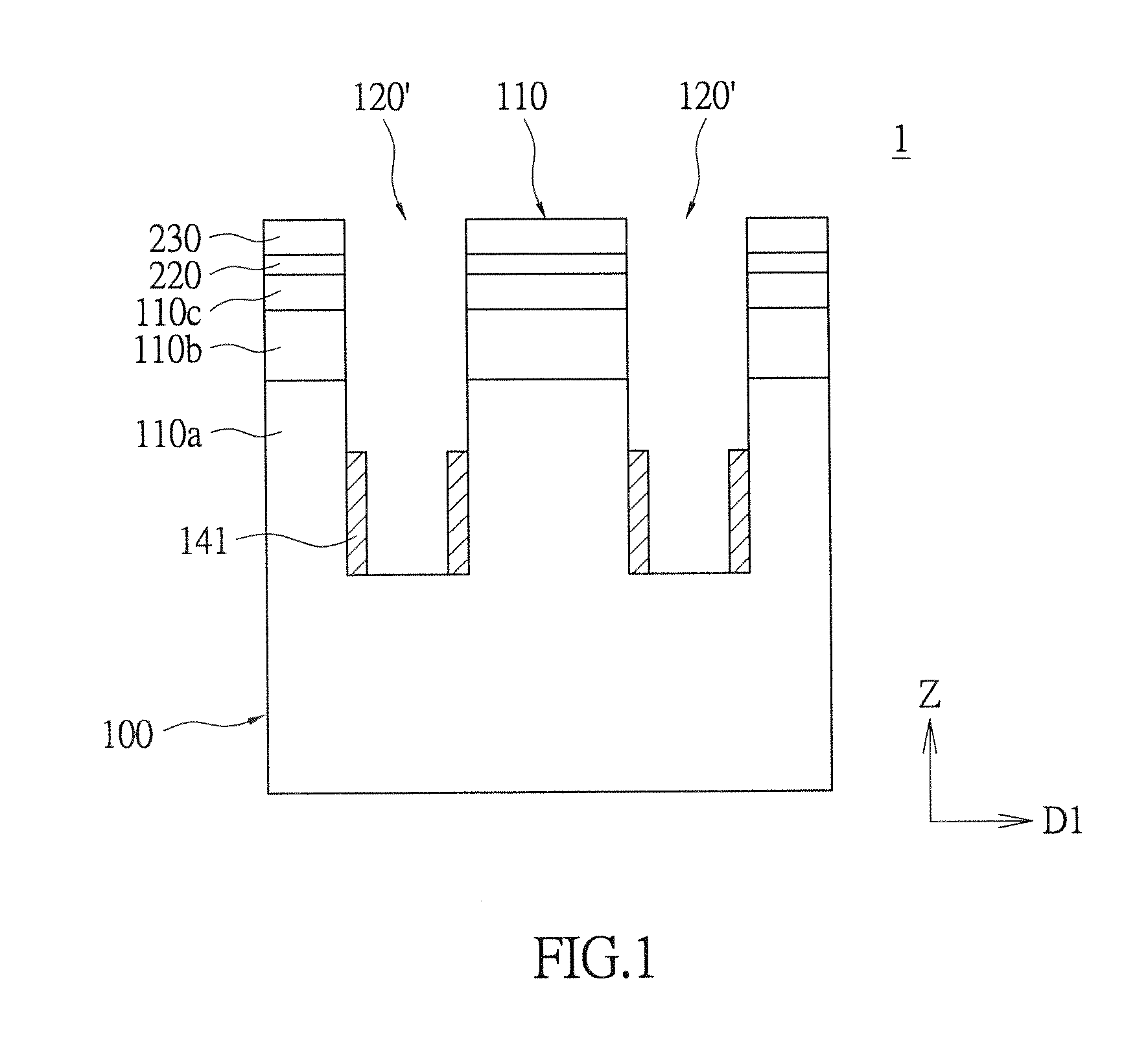
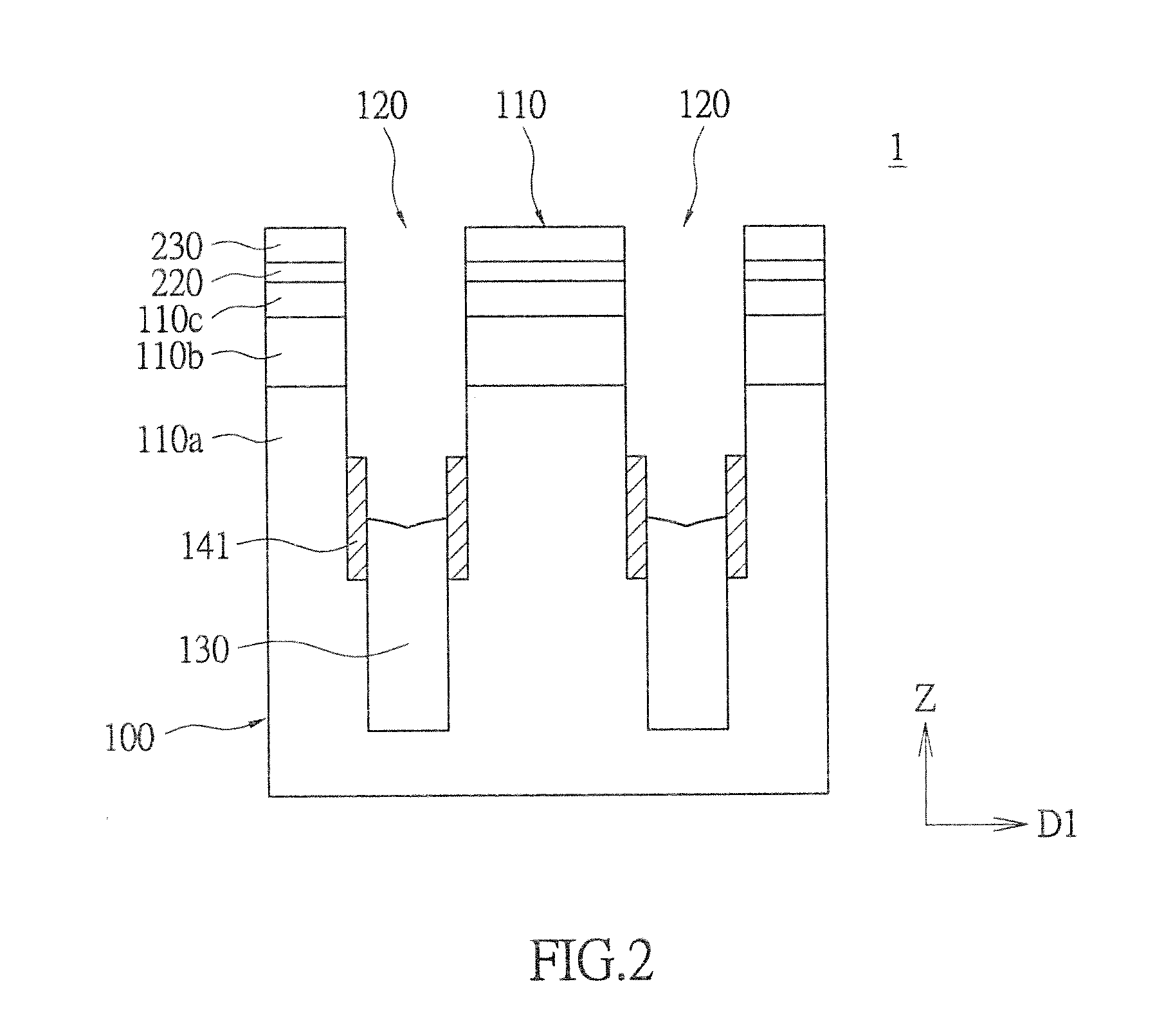
[0017]Please refer to FIG. 5, which illustrates a partial cross-sectional view of a dynamic random access memory structure in accordance with an embodiment of the instant disclosure. As shown in FIG. 5, the dynamic random access memory structure 1 includes a plurality of dynamic random access memory units 10. Each of the dynamic random access memory units 10 includes a substrate 100, a self-aligned trench isolation structure 130, a first trenched gate 140, a first cover layer 150, a gate dielectric layer 160, and a second trenched gate 170. The substrate 100 includes at least one pillar-shaped active body 110 and has a trench 120 disposed therein. The self-alig...


PUM


Abstract

A dynamic random access memory unit includes a substrate having a trench disposed therein, a self-aligned trench isolation structure formed in the bottom portion of the trench, and a first trenched gate formed in the bottom portion of the trench and above the self-aligned trench isolation structure. The substrate includes at least one pillar-shaped active body having a drain region, a body region atop the drain region, and a source region atop the body region. The first trenched gate includes a first spacer formed on the side-wall in the bottom portion of the trench to selectively cover and surround the portion of the side-wall in the trench that comprises the drain region, such for defining the width of the self-aligned trench isolation structure.

Description

BACKGROUND[0001]1. Field of the Invention[0002]The instant disclosure relates to structural arrangement of semiconductor electronic device and fabrication method thereof, and pertains particularly to a semiconductor device having self-aligned trench isolation structure and fabrication method thereof.[0003]2. Description of Related Art[0004]Dynamic Random Access Memory (DRAM) is among the most frequently encountered semiconductor electronic devices today. A DRAM is a type of data storage device that stores bit data in the form of electrical charge in the capacitors thereof. As modern electronic product evolves along the trend of light device-weight and low-physical profile, higher degree of integration and device density of DRAM device becomes a necessary requirement in the effort to achieve further degree of device miniaturization. DRAM, being one of the most commonly used volatile memory device, comprises a plurality of memory cell units. The data / information stored in each memory ...

Claims


Application Information

Patent Timeline
Patent Type & Authority Applications(United States)
IPC IPC(8): H01L27/108H01L21/762H01L29/423H01L29/06H01L29/78
CPCH01L27/10823H01L27/10808H01L21/76224H01L29/7827H01L29/4236H01L29/0653H10B12/315H10B12/318H10B12/377H10B12/34H10B12/395H10B12/0383H10B12/0385H10B12/0387H10B12/0335H10B12/053H10B12/482
Inventor LEE, TZUNG-HAN
Owner MICRON TECH INC
Why Eureka
Try Eureka