Vertical JFET as used for selective component in a memory array

a memory array and vertical jfet technology, applied in the direction of semiconductor devices, electrical apparatus, transistors, etc., can solve the problems of not being particularly suited to the device, and reducing the brightness or brightness of the emitter, so as to facilitate the increase of the density of the memory device, improve the quality of the switching device, and reduce the bulkiness

Inactive Publication Date: 2006-03-09
CYPRESS SEMICON CORP
View PDF11 Cites 15 Cited by
  • Summary
  • Abstract
  • Description
  • Claims
  • Application Information

AI Technical Summary

Benefits of technology

[0008] The present invention provides for systems and methods that facilitate increasing memory device density and improving the quality of switching device(s) employed in polymer memory arrays. According to an aspect of the invention, a vertical JFET can be employed as a switching device in a polymer memory cell array in order to mitigate bulkiness associated with employing typical metal-oxide semiconductor (MOS) devices. This aspect of the invention permits a greater device density in polymer memory cell arrays than previously attainable via employing bulky MOS-type, diode, and / or horizontal JFET devices and mitigates the need for a high-density diode solution to providing a selective component to a memory cell.
[0009] According to another aspect of the invention, critical dimensions of a vertical JFET can be reduced via mitigating all or part of a spacing between a vertical JFET gate and drain. For example, a vertical JFET can be constructed that has no gap between the gate and drain thereof, which facilitates providing a selective component to an associated polymer memory cell while further increasing device density in a polymer memory cell array.

Problems solved by technology

If the device is an LED, application of the voltage may turn the emitter ON or OFF, reduce its brightness or increase its brightness.
MOSFETS, however, can be bulky and thus are not particularly suited to devices wherein high density is a paramount priority in today's semiconductor industry, which strives daily to reduce size and increase capacity of semiconductor devices.

Method used


Image

  • Vertical JFET as used for selective component in a memory array
  • Vertical JFET as used for selective component in a memory array
  • Vertical JFET as used for selective component in a memory array

Examples


Embodiment Construction

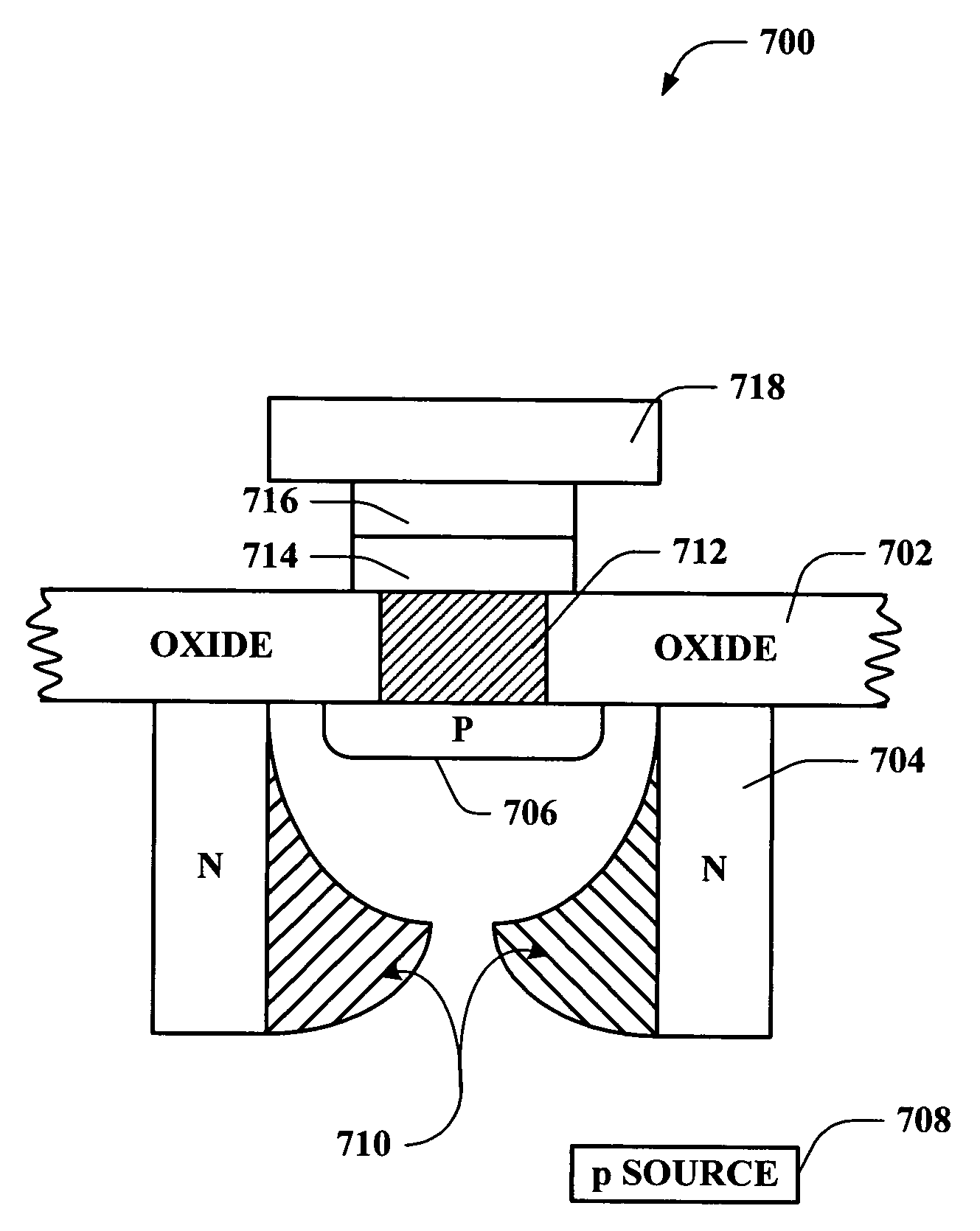
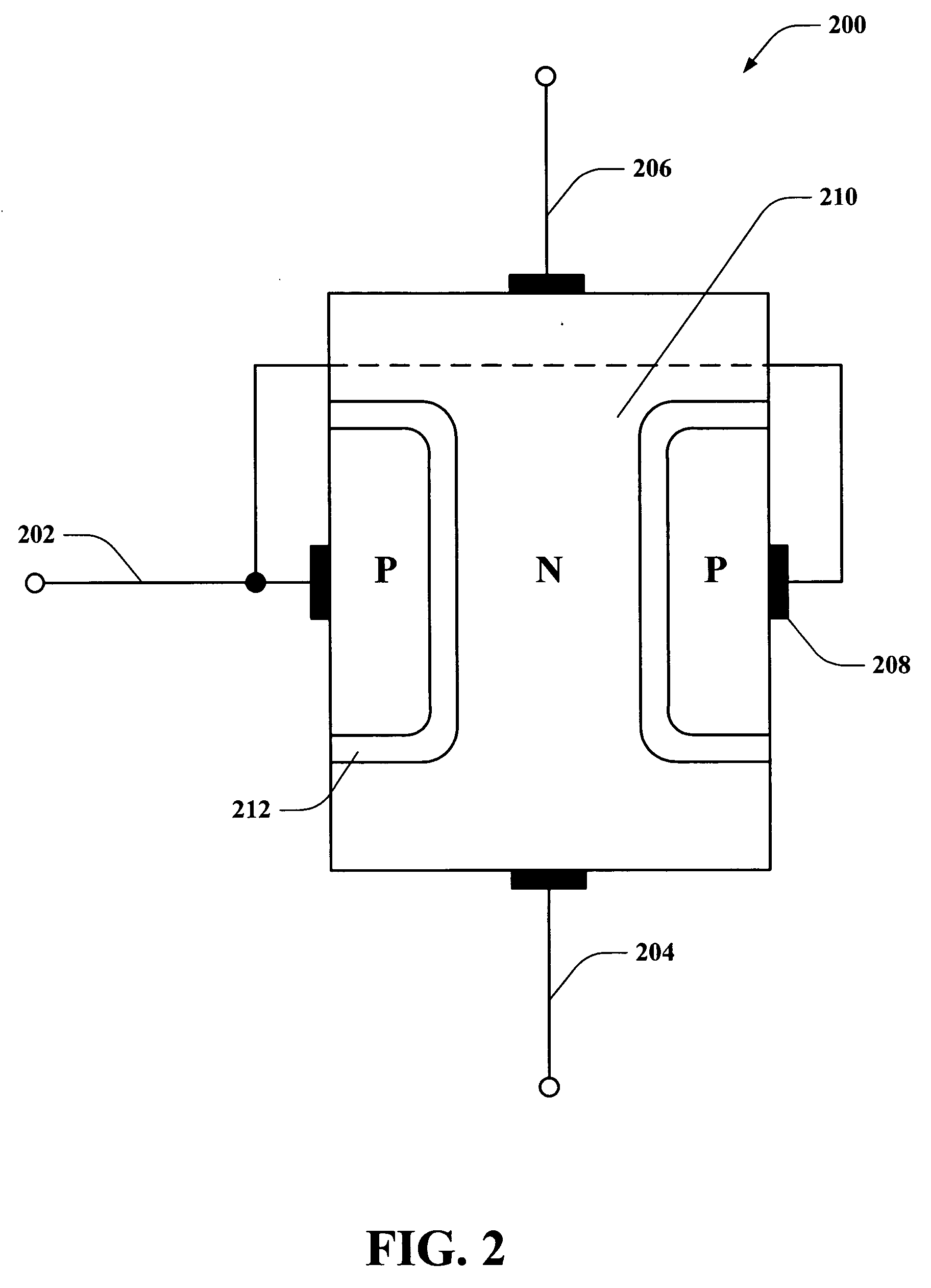
[0024] The present invention will now be described with reference to the drawings, wherein like reference numerals are used to refer to like elements throughout. The present invention will be described with reference to systems and methods increasing memory density and switching device quality in a polymer memory array. It should be understood that the description of these exemplary aspects are merely illustrative and that they should not be taken in a limiting sense.

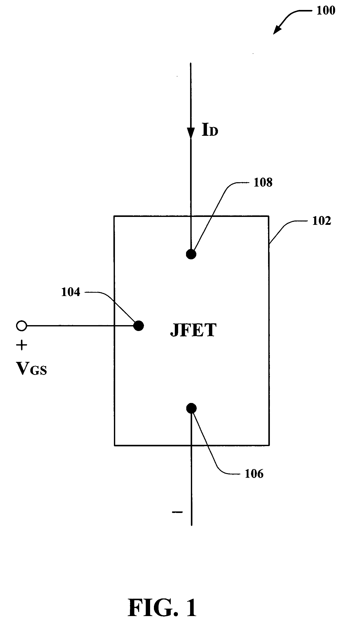
[0025]FIG. 1 is an illustration of a simple junction field-effect transistor (JFET) schematic 100 presented for exemplary purposes and to provide insight into JFET operation. A JFET is a three-terminal device that has numerous applications, many of which comprise providing a functionality similar to, and / or in place of, for example, a bipolar junction transistor (BJT). A FET differs from a BJT in that a BJT is a bipolar, current-controlled device whereas a FET is a unipolar, voltage-controlled device (e.g., amplifier, ...


PUM


Abstract

Systems and methods are disclosed that facilitate providing a selective functionality to a polymer memory cell in a memory array while increasing device density in the memory cell array. A vertical JFET is described to which voltages can be selectively applied to control internal current flow there through, which in turn can be employed to manipulate the state of a polymer memory cell coupled to the vertical JFET. By mitigating gaps between gates, or wordlines, and drains of the vertical JFETs, feature size can be reduced to permit increased device density. Furthermore, vertical JFETs in the array can be coupled to gates on only two opposite sides, permitting the JFETs to be arranged without gate crossbars between them, further increasing device density. In this manner, the present invention provides switching characteristics to a memory cell and overcomes problematic bulkiness associated with conventional MOS devices.

Description

TECHNICAL FIELD [0001] The present invention relates generally to semiconductor fabrication, and more particularly to systems and methodologies that facilitate increased memory density via utilizing vertically oriented JFETs in a memory array. BACKGROUND OF THE INVENTION [0002] In the semiconductor industry, there is a continuing trend toward higher device densities. To achieve these high device densities there have been, and continue to be, efforts toward scaling down device dimensions (e.g., at sub-micron levels) on semiconductor wafers. In order to accomplish such densities, smaller feature sizes and more precise feature shapes are required. This may include width and spacing of interconnecting lines, spacing and diameter of contact holes, and surface geometry, such as corners and edges, of various features. The dimensions of and between such small features can be referred to as critical dimensions (CDs). Reducing CDs and reproducing more accurate CDs facilitates achieving higher...

Claims


Application Information

Patent Timeline
Patent Type & Authority Applications(United States)
IPC IPC(8): H01L29/80
CPCH01L27/10H01L27/098
Inventor BILL, COLIN S.VAN BUSKIRK, MICHAEL A.
Owner CYPRESS SEMICON CORP
Why Eureka
Try Eureka