Optical imaging device

an optical imaging and optical technology, applied in the field of optical imaging devices, can solve the problems of image deformation, inconvenient use of the computer, and increase the cost, and achieve the effect of solving the problem of synchronization of capturing images, saving cost, and low cos

Active Publication Date: 2014-08-05
WISTRON CORP
View PDF13 Cites 6 Cited by
  • Summary
  • Abstract
  • Description
  • Claims
  • Application Information

AI Technical Summary

Benefits of technology

[0020]In summary, the optical imaging device utilizes a plurality of reflective optical units to capture image synchronously by a single image capturing module, so as to save cost and solve an issue of synchronization of capturing images. Furthermore, the present invention utilizes the plurality of reflective optical units to focus the light reflected from the object on a position where the image is captured. Consequently, it can be implemented in large-size display panel neither utilizing an image sensor with a large sensing area nor causing an image to deform. Furthermore, since none of the reflective opticals is disposed within a touch control area of the display panel, it will not cause any inconvenience for a user. The present invention provides the optical imaging device with a low cost, high stability and being capable of solving the issue of synchronization of capturing images.

Problems solved by technology

However, the conventional optical imaging device not only requires more than two image capturing modules so as to detect a shadow formed by the object, but also has an issue of synchronization of capturing images by the two image capturing modules.
Consequently, it results in enhancement of cost.
However, when the display is in large size, it needs the image sensor with a larger sensing area and will cause an issue of image deformation.
Furthermore, since the disposal positions of the reflective mirrors are within the touch control area, it is not convenient for a user to use the computer.
As a result, design of an optical imaging device for reducing cost and being capable of solving the problem of synchronization of capturing images is an important issue of the touch technique.

Method used


Image

  • Optical imaging device
  • Optical imaging device
  • Optical imaging device

Examples


Embodiment Construction

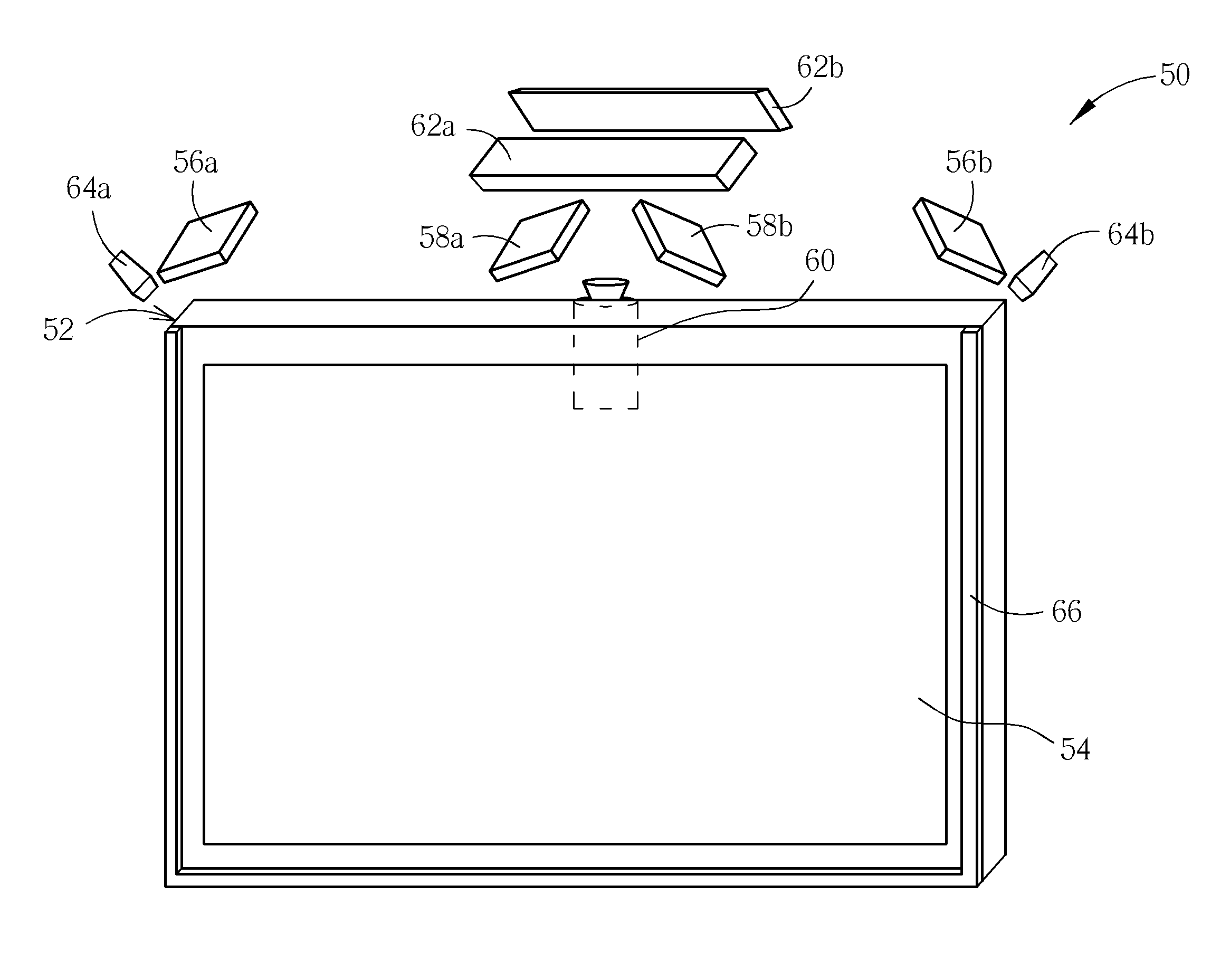
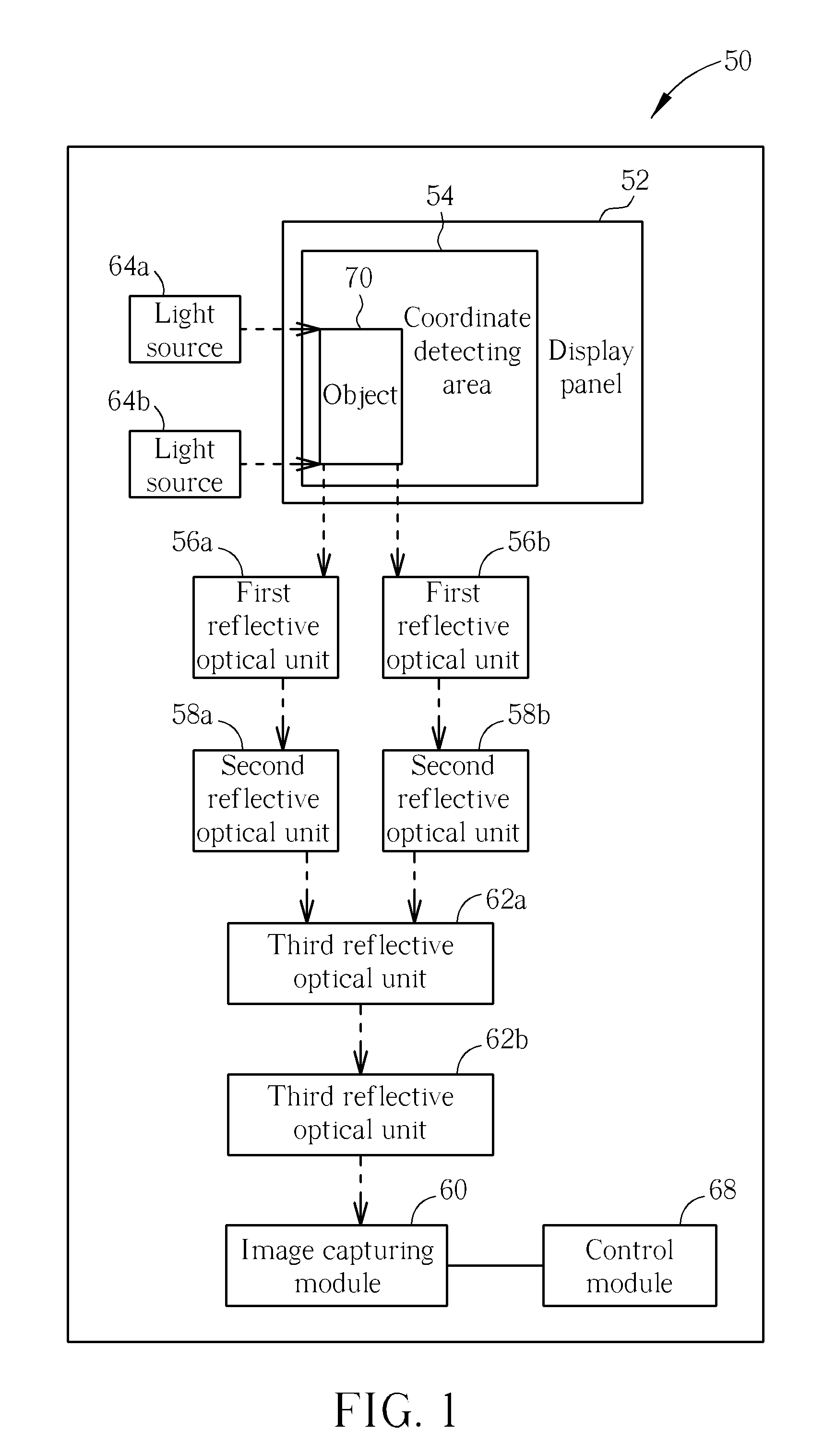
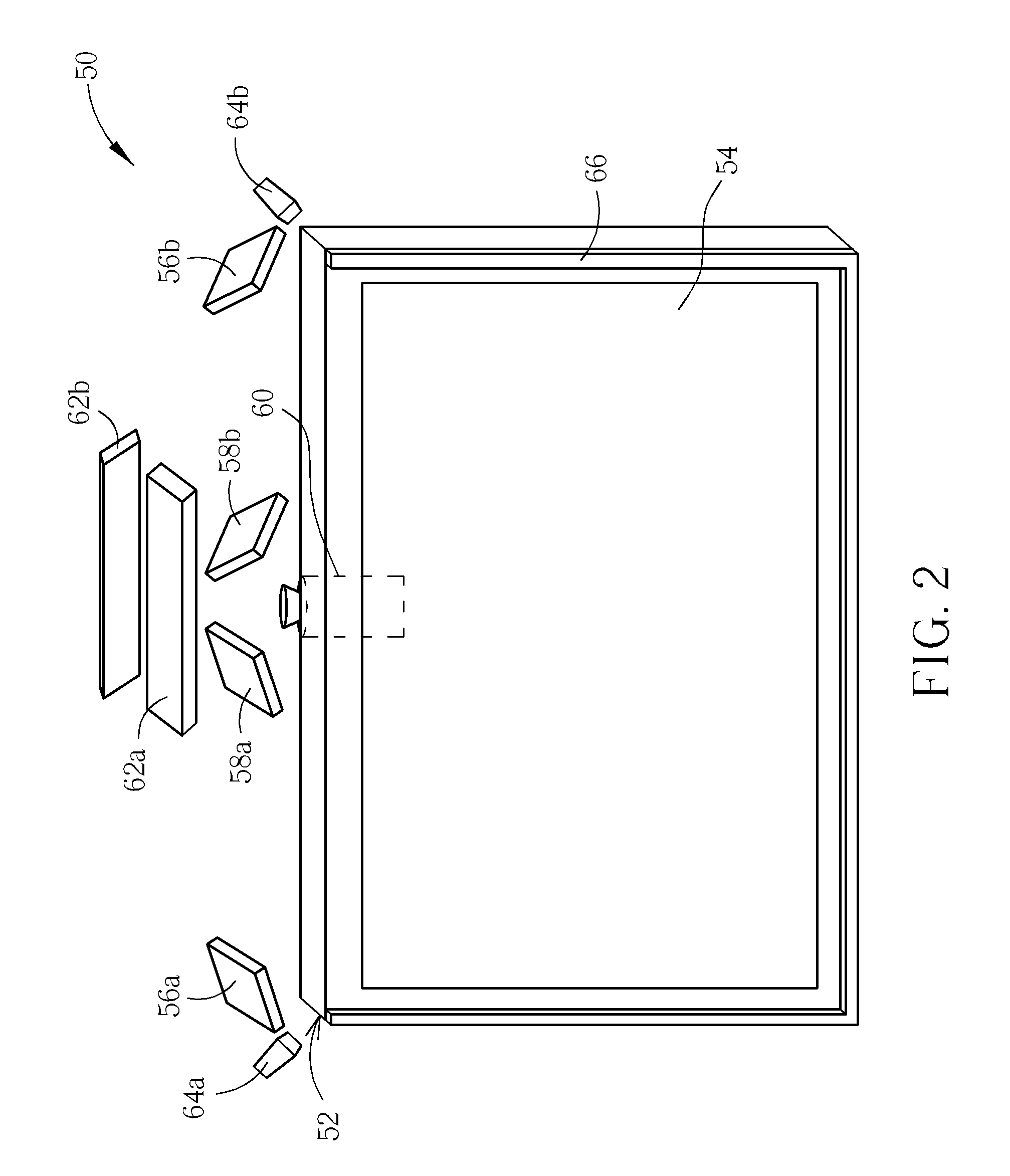
[0028]Please refer to FIG. 1 to FIG. 4. FIG. 1 is a functional block diagram of an optical imaging device 50 according to an embodiment of the present invention. FIG. 2 is a diagram of the optical imaging device 50 according to the embodiment of the present invention. FIG. 3 is a front view of the optical imaging device 50 according to the invention of the present invention. FIG. 4 is a side view of the optical imaging device 50 according to the embodiment of the present invention. The optical imaging device 50 includes a display panel 52 whereon a coordinate detecting area 54 is formed, two first reflective optical units 56a, 56b installed on two outside corners of the display panel 52, two second reflective optical units 58a, 58b installed outside the display panel 52, an image capturing module 60 installed on a side of the display panel 52, two third reflective optical units 62a, 62b disposed on a light path between the second reflective optical unit 58 and the image capturing mo...


PUM


Abstract

An optical imaging device includes a display panel whereon a coordinate detecting area is formed, at least one first reflective optical unit installed on an outside corner of the display panel for reflecting light transmitted from an object moving within the coordinate detecting area, at least one second reflective optical unit installed outside the display panel for reflecting the light reflected from the at least one first reflective optical unit, an image capturing module for capturing the light reflected from the at least one second reflective optical unit so as to capture image of the object, and a control module coupled to the image capturing module for receiving the image captured by the image capturing module and for calculating a coordinate value of the object within the coordinate area according to the image.

Description

BACKGROUND OF THE INVENTION[0001]1. Field of the Invention[0002]The present invention relates to an optical imaging device, and more particularly, to an optical imaging device with a plurality of reflective optical units for capturing image simultaneously by a single image capturing module.[0003]2. Description of the Prior Art[0004]In the modern consumer electronic products market, a portable electronic product such as a personal digital assistant, a smart phone or a mobile phone is equipped with a touch control device as an interface for data transmission. Since consumer electronic products have become lighter, thinner, shorter, and smaller, there is no space on these products for containing a conventional input device, such as a mouse, a keyboard and so on. Furthermore, with development of tablet computers focusing on humanity design, a display with the touch control device has gradually become one of the key components in various electronic products. However, as technology advanc...

Claims


Application Information

Patent Timeline
Patent Type & Authority Patents(United States)
IPC IPC(8): H04N5/225
CPCG06F3/0428
Inventor CHOU, CHIA-TE
Owner WISTRON CORP
Why Eureka
Try Eureka