Power transfer system and noncontact charging device

a technology of power transfer system and charging device, which is applied in the direction of transformers, inductances, transportation and packaging, etc., can solve the problems of unnecessary electric field, increased voltage applied to each electrode, and reduced flexibility of arrangement of both power transmission device and power reception devi

Active Publication Date: 2015-01-20
MURATA MFG CO LTD
View PDF12 Cites 5 Cited by
  • Summary
  • Abstract
  • Description
  • Claims
  • Application Information

AI Technical Summary

Benefits of technology

[0021]According to the above preferred embodiments of the invention, the following advantageous effects may be obtained. The allowance to a relative positional deviation between the power transmission device and the power reception device increases to thereby improve convenience. The degree of coupling between the power transmission device and the power reception device increases, power transfer efficiency may be improved, and the size of the device may be reduced. Because the power transfer efficiency is improved, it is possible to increase an upper limit of electric power that can be transferred. Because the degree of coupling increases, it is possible to decrease a set voltage applied to the central conductor of the power transmission device. In accordance with this, it is possible to decrease the electric potential of the high voltage side conductor of the power reception device. The central conductor is electrostatically shielded by a structure such that the peripheral conductor surrounds the high voltage side conductor, so an unnecessary radiation may be reduced when the conductive layer is configured at the opposite surface of the sheet, and the conductive layer is connected to the ground level.
may be obtained. The allowance to a relative positional deviation between the power transmission device and the power reception device increases to thereby improve convenience. The degree of coupling between the power transmission device and the power reception device increases, power transfer efficiency may be improved, and the size of the device may be reduced. Because the power transfer efficiency is improved, it is possible to increase an upper limit of electric power that can be transferred. Because the degree of coupling increases, it is possible to decrease a set voltage applied to the central conductor of the power transmission device. In accordance with this, it is possible to decrease the electric potential of the high voltage side conductor of the power reception device. The central conductor is electrostatically shielded by a structure such that the peripheral conductor surrounds the high voltage side conductor, so an unnecessary radiation may be reduced when the conductive layer is configured at the opposite surface of the sheet, and the conductive layer is connected to the ground level.

Problems solved by technology

Therefore, there is a problem that the flexibility of arrangement of both the power transmission device and the power reception device is considerably low.
Therefore, there is a problem that a voltage applied to each electrode increases.
Furthermore, because the periphery of each electrode is not shielded, there is a problem that an unnecessary electric field (that does not contribute to power transfer) spreads around the electrodes.
Furthermore, there is a problem that, when alternative voltage of the passive electrode at the power reception device side are large, an electric field also similarly spreads therearound.

Method used


Image

  • Power transfer system and noncontact charging device
  • Power transfer system and noncontact charging device
  • Power transfer system and noncontact charging device

Examples


first embodiment

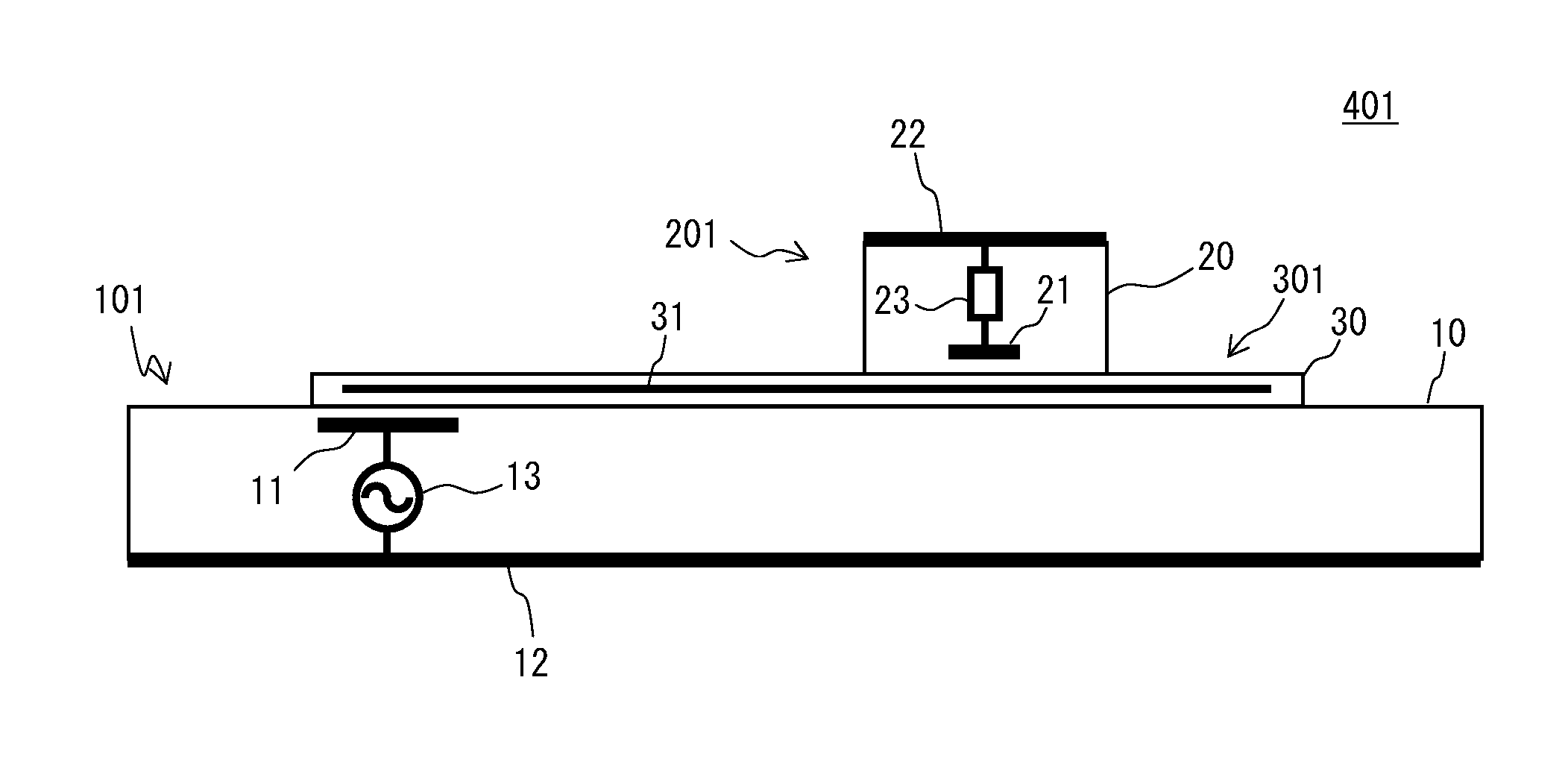
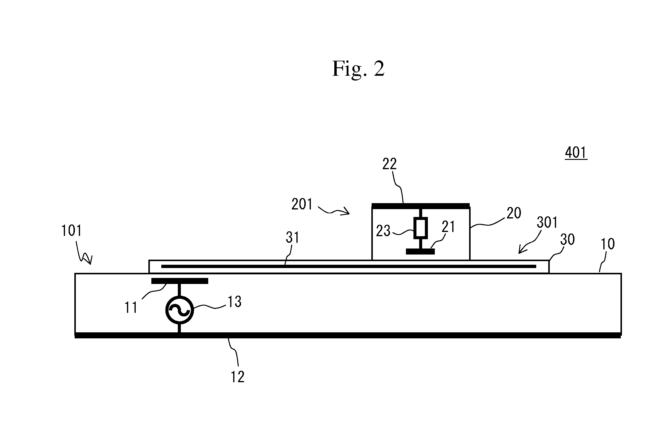
[0039]The configuration of a power transfer system according to a first embodiment will be described with reference to FIG. 2 to FIG. 4. FIG. 2 is a cross-sectional view that conceptually shows a relevant portion of a power transfer system 401. The power transfer system 401 includes a power transmission device 101, a power reception device 201 and an auxiliary sheet 301. A high-voltage side conductor 11 is formed near the upper surface of a casing 10 of the power transmission device 101. A low-voltage side conductor 12 is formed near the lower surface of the casing 10 of the power transmission device 101. In addition, an alternating voltage generating circuit 13 is provided inside the casing 10 of the power transmission device 101 and applies an alternating voltage between the high-voltage side conductor 11 and the low-voltage side conductor 12. In this example, the low-voltage side conductor 12 is widely arranged along the lower surface of the casing 10.

[0040]A high-voltage side co...

second embodiment

[0063]FIG. 7A and FIG. 7B are configuration diagrams of an auxiliary sheet 302 used in a power transfer system according to a second embodiment. FIG. 7A is a top view of the auxiliary sheet 302. FIG. 7B is a cross-sectional view of the auxiliary sheet 302. A capacitive coupling conductor 32 is formed so that a mesh material formed by stamping a metal foil, such as copper foil, is coated with an insulating film, such as resin, foamed material, glass, and ceramics. By forming the inside capacitive coupling conductor 32 in a mesh shape, adhesion between the capacitive coupling conductor 32 and the insulating film improves, thus making it difficult to peel off.

[0064]The configuration of the power transmission device 101 and power reception device 201, other than the auxiliary sheet, is similar to that shown in FIG. 2. In this way, with the mesh capacitive coupling conductor 32, a stray capacitance between the low-voltage side conductor 22 of the power reception device 201 and the capaci...

third embodiment

[0065]FIG. 8A and FIG. 8B are configuration diagrams of an auxiliary sheet used in a power transfer system according to a third embodiment. FIG. 8A is a top view of the auxiliary sheet 303. FIG. 8B is a cross-sectional view of the auxiliary sheet 303. A capacitive coupling conductor 33 is formed so that a metal foil or a mesh conductor, such as copper foil, stamped into a predetermined pattern, is coated with an insulating film, such as resin, foamed material, glass, and ceramics. The configuration of the power transmission device 101 and power reception device 201, other than the auxiliary sheet, is similar to that shown in FIG. 2.

[0066]By holding the capacitive coupling conductor in a predetermined pattern between insulators, it is possible to select the shape of the capacitive coupling conductor 33 interposed between the power transmission device 101 and the power reception device 201 for capacitive coupling. For example, when a position at which the power reception device 201 is...


PUM

PropertyMeasurementUnit
dielectric constantaaaaaaaaaa
relative dielectric constantaaaaaaaaaa
frequencyaaaaaaaaaa

Abstract

A high-voltage side conductor is formed near the upper surface of a power transmission device, and a low-voltage side conductor is formed near the lower surface of the power transmission device. The power transmission device includes an alternating voltage generating circuit. A high-voltage side conductor is formed near the lower surface of a power reception device, and a low-voltage side conductor is formed near the upper surface of the power reception device. The power reception device includes a load circuit. When the high-voltage side conductors face a capacitive coupling conductor of an auxiliary sheet, capacitances are generated respectively between the high-voltage side conductors and the capacitive coupling conductor. Thus, the high-voltage side conductors are capacitively coupled to each other via the capacitive coupling conductor.

Description

CROSS REFERENCE TO RELATED APPLICATIONS[0001]The present application is a continuation of International application No. PCT / JP2009 / 002921, filed Jun. 25, 2009, the entire contents of which is incorporated herein by reference.FIELD OF THE INVENTION[0002]The invention relates to a power transfer system that transfers electric power in a noncontact manner and a noncontact charging device that uses the power transfer system.BACKGROUND OF THE INVENTION[0003]Patent Document 1 and Patent Document 2 describe existing techniques related to a noncontact power transfer system.[0004]The power transfer system described in Patent Document 1 increases the efficiency of power transfer between a card reader / writer and a noncontact-type card. Two electrodes are provided for each of the card reader / writer and the noncontact-type card. When power is transferred, the electrodes of the card reader / writer face the electrodes of the noncontact-type card in a pair to transfer electric power through capaciti...

Claims


Application Information

Patent Timeline
Patent Type & Authority Patents(United States)
IPC IPC(8): H02J7/02H01F27/42H02J7/00
CPCH02J7/025H02J7/0042H02J50/005H02J50/12H02J50/05H02J50/70
Inventor ICHIKAWA, KEIICHIBONDAR, HENRI
Owner MURATA MFG CO LTD
Why Eureka
Try Eureka