Clock generating circuit, semiconductor device including the same, and data processing system

a clock generating circuit and clock technology, applied in the direction of digital storage, pulse automatic control, instruments, etc., can solve the problems of reducing the performance of the semiconductor device, and continuously consuming certain power, so as to achieve the effect of reducing the power consumption during the phase control operation

Active Publication Date: 2015-04-14
LONGITUDE LICENSING LTD
View PDF33 Cites 3 Cited by
  • Summary
  • Abstract
  • Description
  • Claims
  • Application Information

AI Technical Summary

Benefits of technology

[0011]According to the present invention, when a first clock signal that is an output of a clock generating unit attains a predetermined phase, the phase of the first clock signal is fixed, and therefore power consumption during a phase control operation can be reduced. Further, because the phase control operation is restarted in response to a trigger signal, the phase of the internal clock signal is not likely to significantly deviate from a desired phase.

Problems solved by technology

Thus, certain power is continuously consumed even after the DLL circuit is locked.
However, when the power supply to the DLL circuit is stopped, the count value of a counter circuit is disadvantageously reset.
Therefore, the DLL circuit cannot be accessed until the DLL circuit is relocked after the power supply to the DLL circuit is restarted, and this leads to a decrease in the performance of the semiconductor device.
Because the operation of the DLL circuit is continued until a refresh command is issued, the power consumption by the DLL circuit cannot be reduced during this period.
Such problems occur not only in DLL circuits but it also commonly occurs in clock generating circuits that generate a phase-controlled internal clock signal.

Method used


Image

  • Clock generating circuit, semiconductor device including the same, and data processing system
  • Clock generating circuit, semiconductor device including the same, and data processing system
  • Clock generating circuit, semiconductor device including the same, and data processing system

Examples


first embodiment

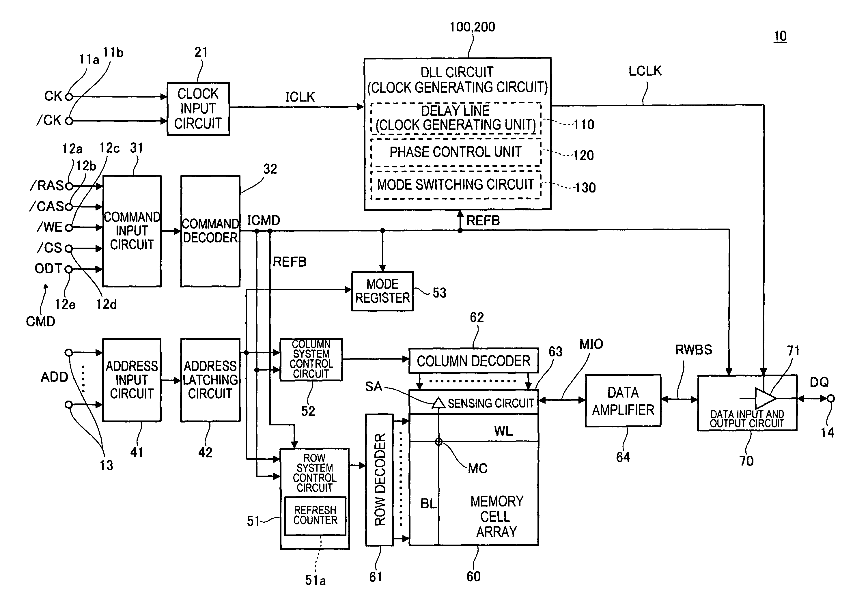
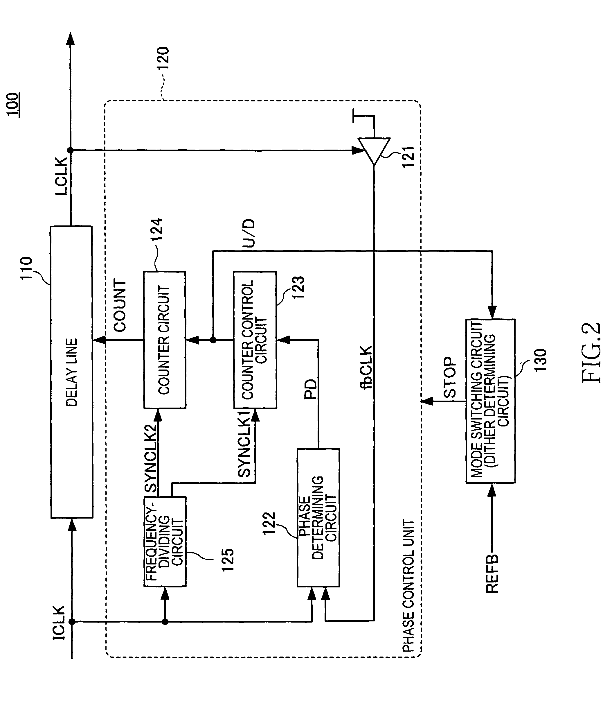
[0037]FIG. 2 is a block diagram of the DLL circuit 100 according to the present invention.

[0038]As shown in FIG. 2, the DLL circuit 100 includes the delay line (the clock generating unit) 110, the phase control unit 120, and the mode switching circuit 130.

[0039]The delay line 110 is a circuit that generates an internal clock signal LCLK for output by delaying the internal clock signal ICLK. The phase control unit 120 adjusts an amount of delay of the delay line 110. Although the configuration thereof is not particularly limited, the delay line 110 preferably includes a coarse delay line that delays the internal clock signal ICLK at a relatively coarse adjustment pitch, and a fine delay line that delays the internal clock signal ICLK at a relatively fine adjustment pitch.

[0040]The phase control unit 120 is a circuit block that receives the internal clock signal ICLK and the internal clock signal LCLK for output. By adjusting the amount of delay of the delay line 110 based on these re...

second embodiment

[0058]the present invention is explained next.

[0059]FIG. 5 is a block diagram of the DLL circuit 200 according to the second embodiment.

[0060]The DLL circuit 200 according to the second embodiment differs from the DLL circuit 100 according to the first embodiment in the following aspects. That is, in the second embodiment, the phase control unit 120 and the mode switching circuit 130, respectively, are replaced by a phase control unit 220 and a mode switching circuit 230. Furthermore, the phase control unit 220 differs from the phase control unit 120 shown in FIG. 2, in that it includes a frequency-dividing circuit 225 instead of the frequency-dividing circuit 125. The DLL circuit 200 is identical to the DLL circuit 100 in all other respects. Therefore, like reference numerals are denoted to like elements and redundant explanations thereof will be omitted.

[0061]In addition to the sampling clock signals SYNCLK1 and SYNCLK2, the frequency-dividing circuit 225 generates a set signal SE...

third embodiment

[0075]the present invention is explained next.

[0076]FIG. 8 is a block diagram of a configuration of a semiconductor device 10a according to the third embodiment.

[0077]The semiconductor device 10a according to the third embodiment differs from the semiconductor device 10 shown in FIG. 1, in that it includes a voltage variation detecting circuit 300 and an AND gate 301. The semiconductor device 10a is identical to the semiconductor device 10 shown in FIG. 1 in all other aspects. Therefore, like reference numerals are denoted to like elements and redundant explanations thereof will be omitted.

[0078]The voltage variation detecting circuit 300 is a circuit that causes a detection signal J3 to activate when it detects variation in power supply voltage. The generated detection signal J3 and the refresh signal REFB are input into the AND gate 301. In the third embodiment, an output of the AND gate 301 is used as the stop signal STOP, and it is supplied to the DLL circuit 100 or 200.

[0079]FI...


PUM


Abstract

A clock generating circuit includes a delay line that generates an internal clock signal, a phase-controlling unit that adjusts a phase of the internal clock signal by controlling the delay line, and a mode switching circuit that switches an operation mode of the phase-controlling unit. The phase-controlling unit has a first operation mode in which a phase of the internal clock signal is changed in synchronization with a sampling clock signal and a second operation mode in which the phase of the internal clock signal is fixed. The mode switching circuit shifts the phase-controlling unit to the first operation mode in response to a trigger signal, such as a refresh signal, and, shifts the phase-controlling unit to the second operation mode in a state where the internal clock signal attains a predetermined phase.

Description

BACKGROUND OF THE INVENTION[0001]1. Field of the Invention[0002]The present invention relates to a clock generating circuit and a semiconductor device including the same, and more particularly relates to a clock generating circuit that generates, similarly to a DLL (Delay Locked Loop) circuit, a phase-adjusted internal clock signal, and a semiconductor device including the same. The present invention also relates to a data processing system including such a semiconductor device.[0003]2. Description of Related Art[0004]In recent years, a synchronous memory that performs operations in synchronization with a clock has been widely used for a main memory of a personal computer or the like. Specifically, in a DDR (Double Data Rate) synchronous memory, because an input data and an output data need to be synchronized correctly with respect to an external clock signal, it becomes necessary to provide a DLL circuit that generates an internal clock signal that is synchronized with the external...

Claims


Application Information

Patent Timeline
Patent Type & Authority Patents(United States)
IPC IPC(8): G11C7/00H03L7/06G11C7/10G11C7/22H03L7/081H03L7/095
CPCG11C7/22G11C7/1066G11C7/1093G11C7/222H03L7/0814H03L7/0816H03L7/095H03L7/0818G11C11/406H03L7/0802H03L7/081
Inventor MIYANO, KAZUTAKA
Owner LONGITUDE LICENSING LTD
Why Eureka
Try Eureka