Electronic component

a technology of electronic components and components, applied in the direction of fixed capacitor details, printed circuit non-printed electric components association, final product manufacturing, etc., can solve the problems of difficult to achieve changes to land patterns for circuit boards currently used, circuit boards that vibrate, and multilayer ceramic capacitors subject to mechanical distortion in some cases, so as to reduce the adhesion of bonding agents, reduce the effect of adhesion and large distortion

Active Publication Date: 2015-05-26
MURATA MFG CO LTD
View PDF10 Cites 3 Cited by
  • Summary
  • Abstract
  • Description
  • Claims
  • Application Information

AI Technical Summary

Benefits of technology

[0009]Accordingly, preferred embodiments of the present invention provide an electronic component that allows easy structural design and mounting, and has a mounting strength and electrical characteristics equivalent to those of mounting structures of the related art.
[0011]According to this configuration, each of the grooves is located in a side surface of the substrate. Therefore, for example, in a case where the electronic component is mounted onto the circuit board with a bonding agent such as a solder, the amount of bonding agent that is allowed to escape to the grooves increases, thus reducing the amount of bonding agent that climbs and wets onto the front surface electrodes. As a result, in a case where the chip component undergoes distortion due to variations in applied voltage, it is possible to reduce adhesion of the bonding agent to a region in which the distortion has occurred.
[0013]In this case, as opposed to a case where four grooves are provided, the amount of bonding agent that climbs and wets onto the front surface electrodes is further reduced. As a result, in a case where the chip component undergoes distortion due to variations in applied voltage, it is possible to reduce adhesion of the bonding agent to a region in which the distortion has occurred so as to reduce or prevent connection failures.
[0015]According to this configuration, each of the front surface electrodes includes two flat electrodes, and the two flat electrodes are provided on the front surface of the substrate so as to be spaced apart from each other. For example, in a case where the chip component is a multilayer ceramic capacitor including inner electrodes that are perpendicular or substantially perpendicular to the front surface of the substrate, by providing a space between the two flat electrodes, when the inner electrodes undergo changes due to applied voltage, the portion that undergoes large changes is located between the two flat electrodes so as to prevent the portion that has undergone changes from coming into contact with the flat electrodes.
[0017]According to this configuration, by controlling the direction in which to mount the multilayer ceramic capacitor, it is possible to reduce adhesion of a bonding agent made of a solder or the like to a region of the chip component which is subject to large distortion due to variations in applied voltage. Moreover, a flat substrate is preferably used, and the multilayer ceramic capacitor is mounted on the substrate. Therefore, structural design and mounting are easy, and a mounting strength and electrical characteristics equivalent to those of mounting structures commonly used in related art is achieved.
[0018]When the multilayer ceramic capacitor is mounted onto the circuit board by using the electronic component according to one of the preferred embodiments of the present invention, a defect in the bond created by the bonding agent at the time of mounting is significantly reduced or prevented. In addition, the electronic component has a simple structure and allows miniaturization, and allows easy mounting onto the circuit board. Furthermore, it is possible to ensure a mounting strength and electrical characteristics equivalent to those of mounting structures commonly used in related art.

Problems solved by technology

However, a multilayer ceramic capacitor is subject to mechanical distortion in some cases due to variations in the voltage applied to the multilayer ceramic capacitor.
When this distortion occurs, the distortion is transmitted to the circuit board, causing the circuit board to vibrate.
However, such changes to the land pattern are difficult to achieve for circuit boards currently used which typically require high-density mounting.

Method used


Image

  • Electronic component
  • Electronic component
  • Electronic component

Examples


Embodiment Construction

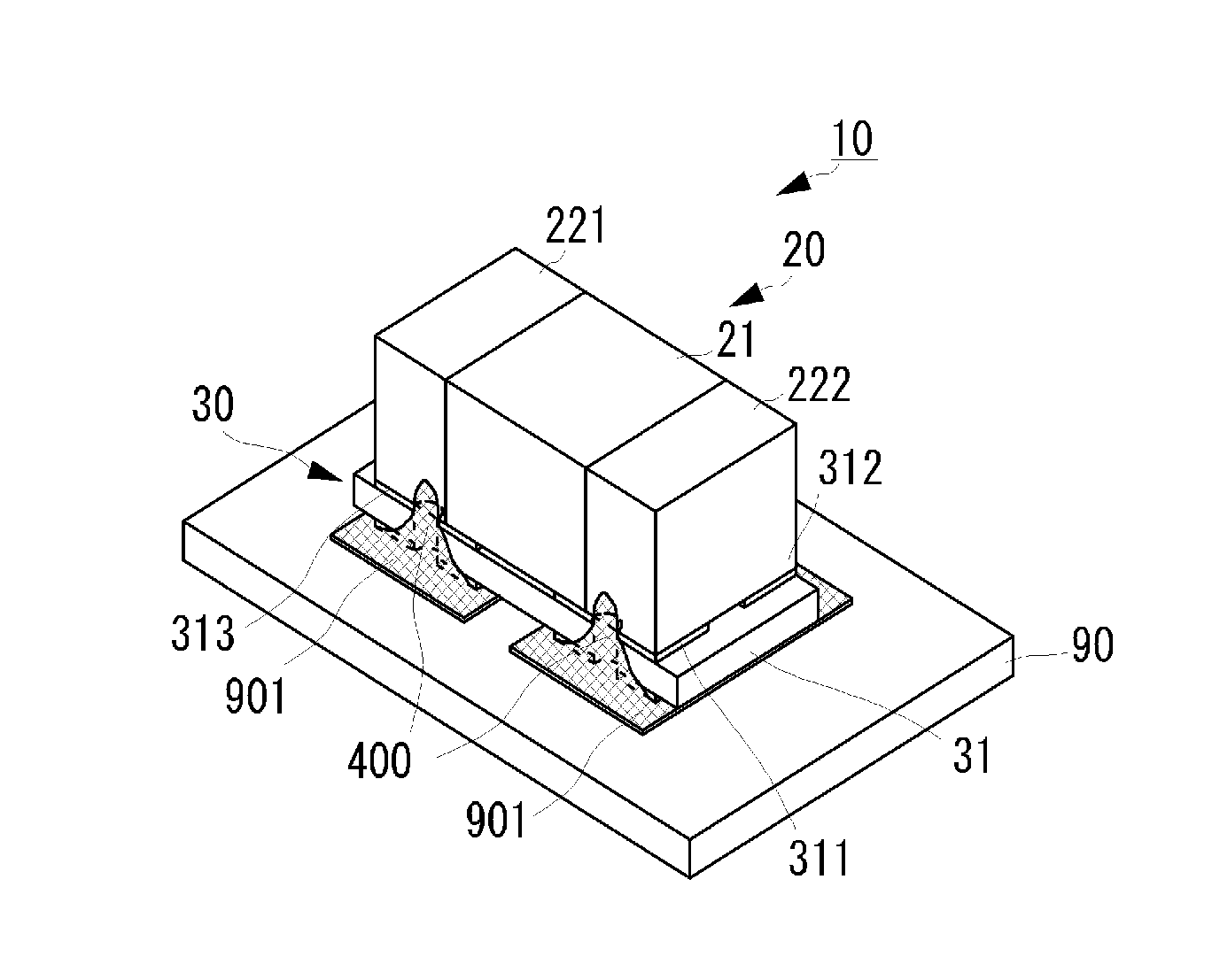
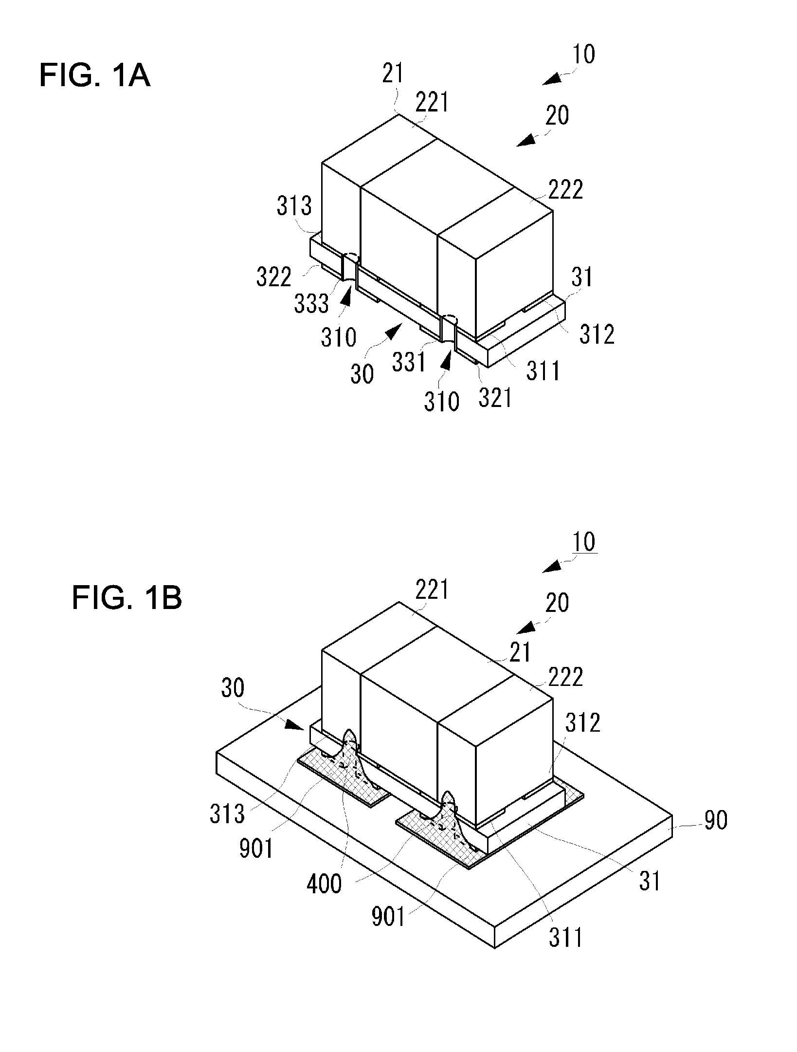
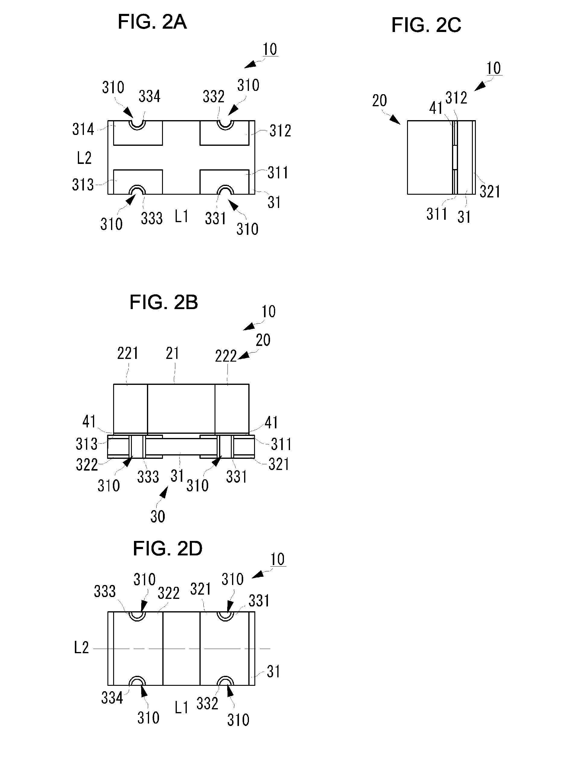
[0025]An electronic component according to a preferred embodiment of the present invention will be described with reference to the drawings. FIG. 1A is a perspective view of the outward appearance of an electronic component 10 according to a preferred embodiment of the present invention. FIG. 1B is a perspective view of the mounting state of the electronic component 10. FIGS. 2A-2D are four-side views of the electronic component 10 according to the present preferred embodiment, of which FIG. 2A is a plan view, FIG. 2B is a first (longitudinal) side view, FIG. 2C is a second (lateral) side view, and FIG. 2D is a rear view. FIGS. 3A and 3B are a first side view and a second side view each illustrating the mounting state of the electronic component 10 according to the present preferred embodiment.

[0026]The electronic component 10 includes a multilayer ceramic capacitor (chip component) 20 and an interposer 30. In FIG. 2A, the multilayer ceramic capacitor 20 that is mounted on the subst...


PUM


Abstract

An electronic component includes an interposer, and a multilayer ceramic capacitor. The interposer includes a substrate including front and back surfaces that are parallel or substantially parallel to each other. Two first mounting electrodes and two second mounting electrodes are located on the front surface of the substrate, on opposite end portions in the longitudinal direction. Recesses are located in the longitudinal side surface of the insulating substrate. Connecting conductors are each provided in the side wall surface of each of the recesses. The connecting conductors connect a first external connection electrode and a second external connection electrode that are located on the back surface of the substrate, and first mounting electrodes and second mounting electrodes.

Description

BACKGROUND OF THE INVENTION[0001]1. Field of the Invention[0002]The present invention relates to an electronic component including a multilayer ceramic capacitor, and an interposer used when mounting the multilayer ceramic capacitor onto a circuit board.[0003]2. Description of the Related Art[0004]Currently, chip components, in particular, miniature multilayer ceramic capacitors are frequently used for mobile terminals such as cellular phones. A multilayer ceramic capacitor includes a rectangular component body that functions as a capacitor, and outer electrodes formed at opposite ends of the component body.[0005]In related art, generally, as disclosed in Japanese Unexamined Patent Application Publication No. 8-55752, a multilayer ceramic capacitor is electrically and physically connected to a circuit board by placing outer electrodes directly on the mounting land of the circuit board of a mobile terminal, and bonding the mounting land and the outer electrodes together with a bondin...

Claims


Application Information

Patent Timeline
Patent Type & Authority Patents(United States)
IPC IPC(8): H05K7/00H05K1/11H05K1/16H01G2/06H01G4/228H05K1/18H05K3/34
CPCH05K1/181H01G2/065H05K3/3442H01G4/228H05K2201/049H05K2201/09181H05K2201/10636Y02P70/50
Inventor HATTORI, KAZUOFUJIMOTO, ISAMU
Owner MURATA MFG CO LTD
Why Eureka
Try Eureka