
Light emitting diode with high light extraction efficiency and method for manufacturing the same

a light-emitting diode and high-efficiency technology, applied in semiconductor/solid-state device manufacturing, semiconductor devices, electrical devices, etc., can solve the problem of decreasing the light-emitting diode's light extraction efficiency

Inactive Publication Date: 2015-06-09
ADVANCED OPTOELECTRONIC TECH INC
View PDF20 Cites 0 Cited by
  • Summary
  • Abstract
  • Description
  • Claims
  • Application Information

AI Technical Summary

Benefits of technology

[0005]Generally, to achieve a homogenous current distribution in the semiconductor layers without decreasing light extraction efficiency thereof, a transparent indium tin oxide (ITO) layer is formed between the P-type electrode and the P-type semiconductor layer. A transparent protecting layer is further formed on the transparent conductive layer to protect the light emitting diode. However, in fact, both the transparent conductive layer and the transparent protecting layer will result in total reflection when the light exits therefrom, thereby decreasing light extraction efficiency of the light emitting diode.

Problems solved by technology

However, in fact, both the transparent conductive layer and the transparent protecting layer will result in total reflection when the light exits therefrom, thereby decreasing light extraction efficiency of the light emitting diode.

Method used


Image

  • Light emitting diode with high light extraction efficiency and method for manufacturing the same
  • Light emitting diode with high light extraction efficiency and method for manufacturing the same
  • Light emitting diode with high light extraction efficiency and method for manufacturing the same

Examples


Embodiment Construction

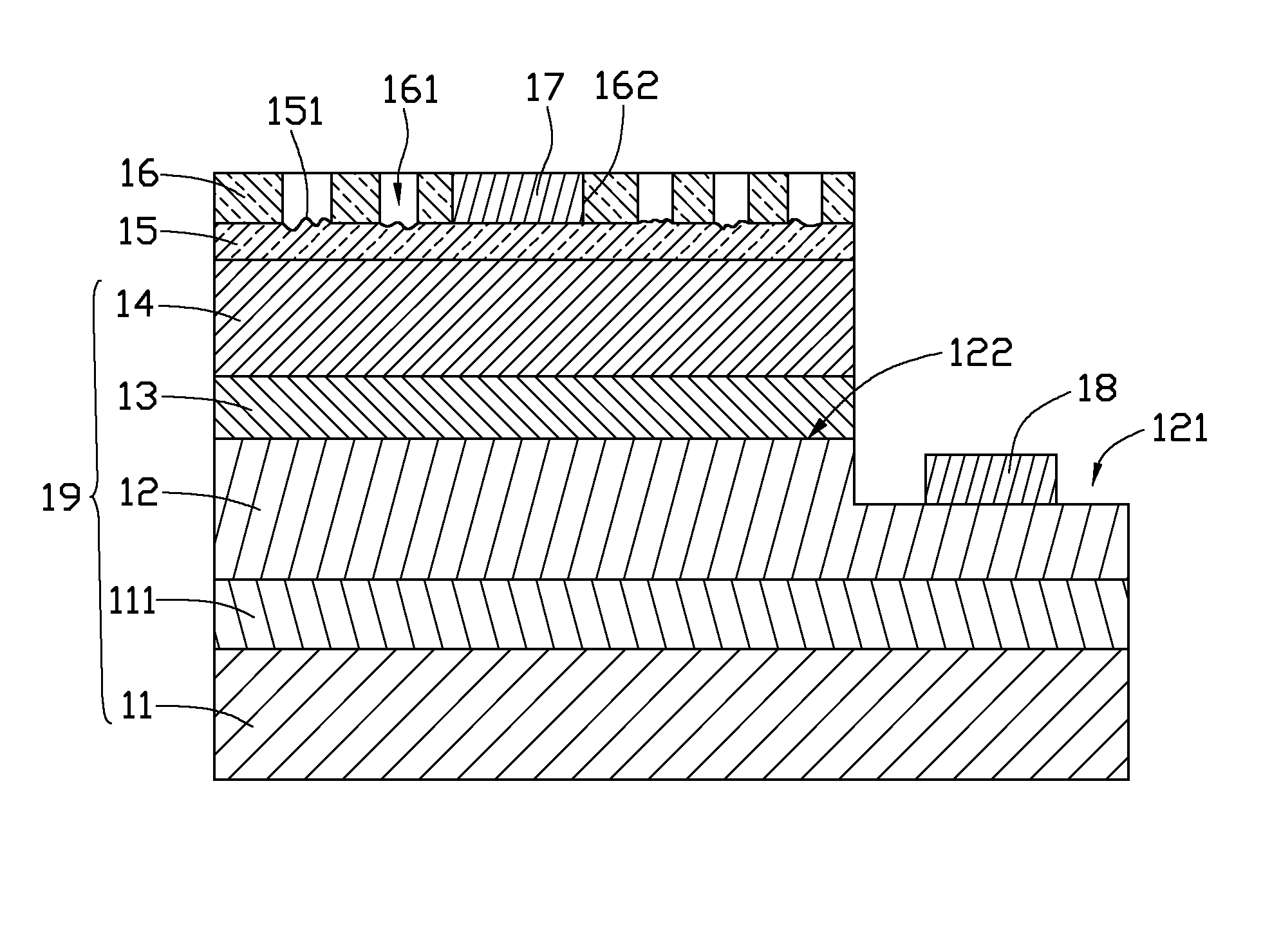
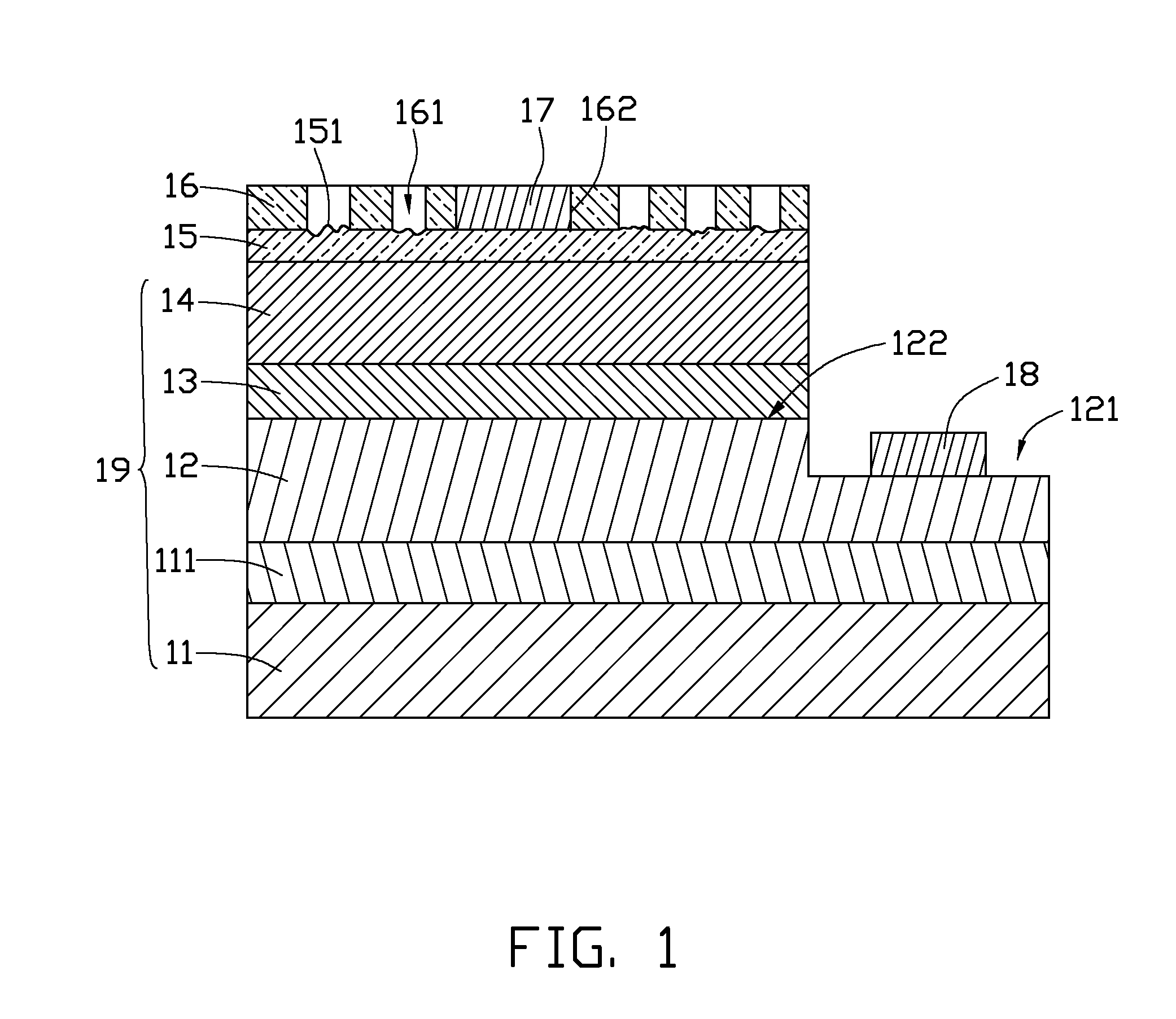
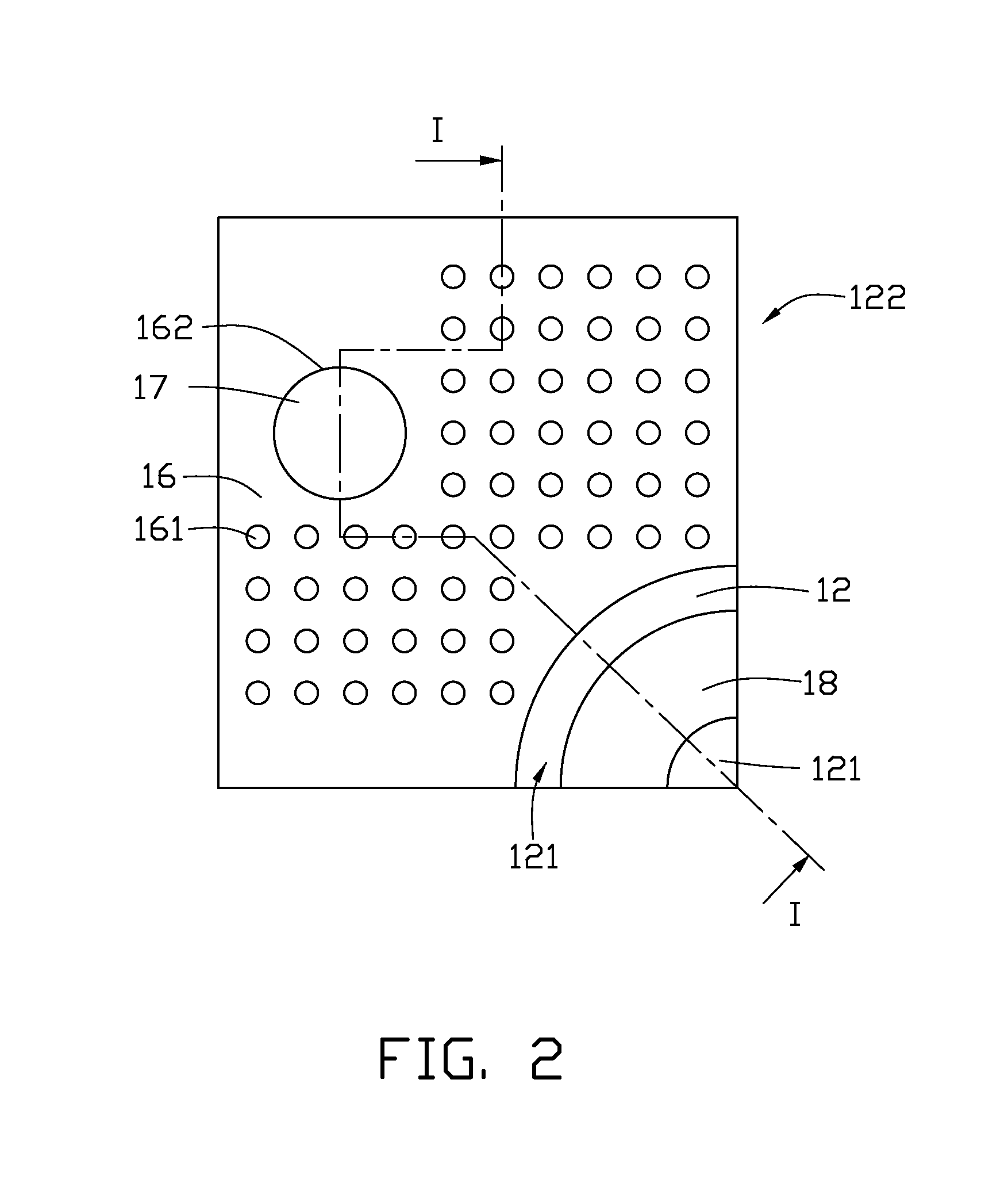
[0013]Referring to FIG. 1, a light emitting diode 10 in accordance with a first exemplary embodiment is provided. The light emitting diode 10 includes a light emitting structure 19, a transparent conductive layer 15, a transparent protecting layer 16, a first electrode 17 and a second electrode 18 having an opposite polarity with respect to the first electrode 17. The light emitting structure 19 includes a substrate 11, a first-type semiconductor layer 12, an active layer 13, and a second-type semiconductor layer 14. The transparent conductive layer 15 is transparent to light and conductive to electricity.

[0014]The substrate 11 is dielectric. The substrate 11 can be sapphire (α-Al2O3) substrate, silicon carbide (SiC) substrate, etc.

[0015]The first-type semiconductor layer 12, the active layer 13 and the second-type semiconductor layer 14 are formed on the substrate 11 in sequence, from bottom to top. Before formation of the first-type semiconductor 12, a buffer layer 111 which can l...


PUM


Abstract

A light emitting diode includes a light emitting structure, a transparent conductive layer and a transparent protecting layer formed in sequence. A plurality of holes are defined in the transparent protecting layer to expose the transparent conductive layer out of the transparent protecting layer. A plurality of micro-structures are formed on a top surface of the transparent conductive layer in the holes. The micro-structures refract light emitted from the light emitting structure and travelling through the transparent conductive layer.

Description

BACKGROUND[0001]1. Technical Field[0002]The disclosure relates to light emitting diodes, and particularly to a light emitting diode with a transparent protecting layer and a transparent conductive layer whose structures are modified to thereby increase light extraction efficiency of the light emitting diode, and a method for manufacturing the light emitting diode.[0003]2. Description of the Related Art[0004]A conventional light emitting diode (LED) includes a substrate, a light emitting structure having an N-type semiconductor layer, an active layer and a P-type semiconductor layer formed on the substrate in sequence, and two electrodes (i.e., N-type and P-type electrodes) respectively connected to the N-type and P-type semiconductor layers. There are several factors affecting the light extraction efficiency of the light emitting diode, such as material of the semiconductor layer, construction of the light emitting structure, transparency of the light emitting diode, or total reflec...

Claims


Application Information

Patent Timeline
Patent Type & Authority Patents(United States)
IPC IPC(8): H01L33/00H01L33/60H01L33/62H01L33/38H01L33/42H01L33/20H01L33/54H01L33/44
CPCH01L33/42H01L33/60H01L33/62H01L33/20H01L33/38H01L33/54H01L33/44H01L2933/0091
Inventor LIU, CHIH-JUNGHUNG, TZU-CHIEN
Owner ADVANCED OPTOELECTRONIC TECH INC
Learn More