
Method for producing substrate for semiconductor light emitting elements, method for manufacturing semiconductor light emitting element, substrate for semiconductor light emitting elements, and semiconductor light emitting element

a technology which is applied in the direction of basic electric elements, electrical devices, semiconductor devices, etc., can solve the problem and achieve the effect of reducing the light extraction efficiency of semiconductor light emitting elements

Active Publication Date: 2018-03-06
OJI HLDG CORP
View PDF22 Cites 0 Cited by
  • Summary
  • Abstract
  • Description
  • Claims
  • Application Information

AI Technical Summary

Benefits of technology

The present disclosure provides a method for manufacturing a substrate for semiconductor light emitting elements that improves the light extraction efficiency. This is achieved by reducing total reflection of light at the interface between the light emitting structure and the substrate. Additionally, a film can be easily formed on the substrate for semiconductor light emitting elements while reducing crystal defects and improving the light extraction efficiency.

Problems solved by technology

If such total reflection is repeated, the light produced in the light emitting structure will attenuate within the light emitting structure, which reduces the light extraction efficiency of the semiconductor light emitting element.

Method used


Image

  • Method for producing substrate for semiconductor light emitting elements, method for manufacturing semiconductor light emitting element, substrate for semiconductor light emitting elements, and semiconductor light emitting element
  • Method for producing substrate for semiconductor light emitting elements, method for manufacturing semiconductor light emitting element, substrate for semiconductor light emitting elements, and semiconductor light emitting element
  • Method for producing substrate for semiconductor light emitting elements, method for manufacturing semiconductor light emitting element, substrate for semiconductor light emitting elements, and semiconductor light emitting element

Examples


first embodiment

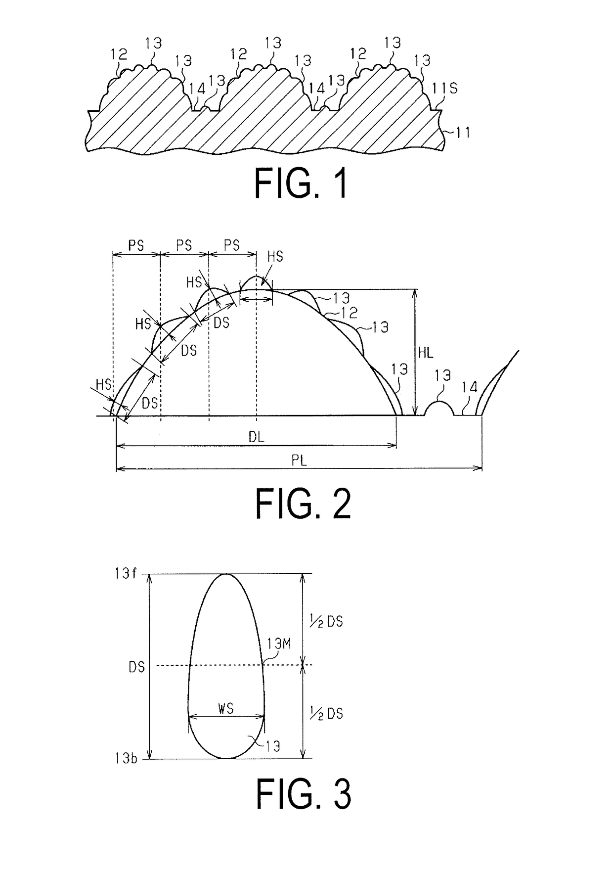
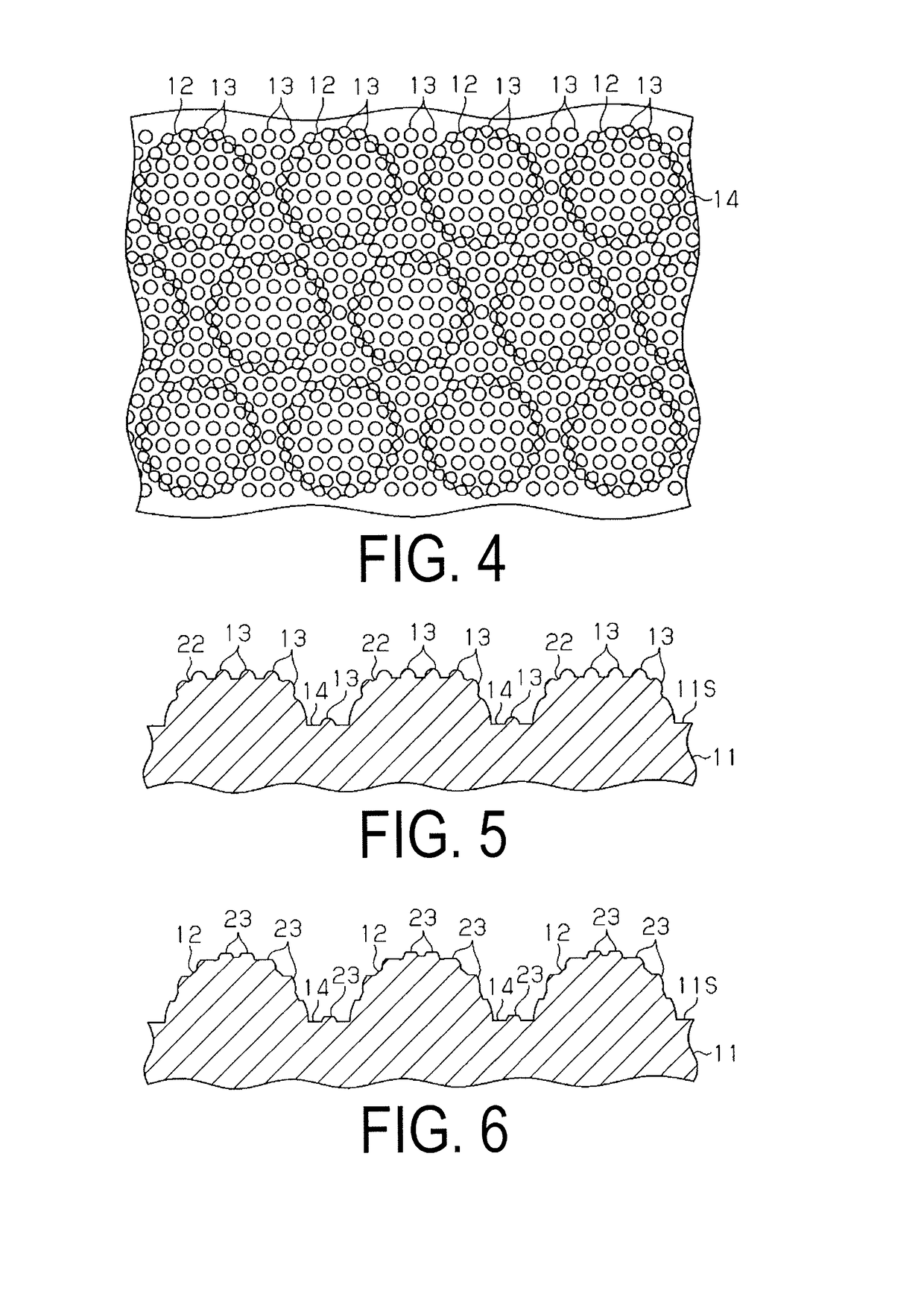
[0082]Referring to FIGS. 1 to 4, an embodiment of a substrate for semiconductor light emitting elements will be described as a first embodiment of the technique of the present disclosure.

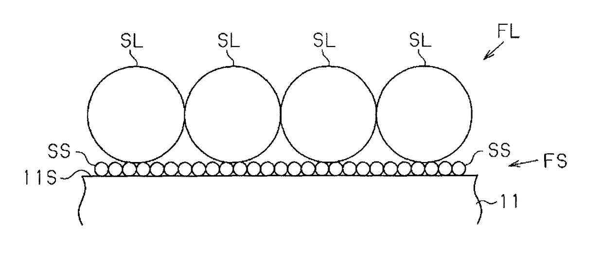
[0083]As illustrated in FIG. 1, an element substrate 11, which is a substrate for semiconductor light emitting elements, has a light emitting structure formation surface 11S as one of the surfaces of the substrate. A light emitting structure is formed on the light emitting structure formation surface 11S during a process for manufacturing the semiconductor light emitting element.

[0084]The material of which the element substrate 11 is formed has thermal, mechanical, chemical, and optical resistance in the process for manufacturing the semiconductor light emitting element. The material of which the element substrate 11 is formed is one selected from the group consisting of, for example, Al2O3 (sapphire), SiC, Si, Ge, MgAl2O4, LiTaO3, LiNbO3, ZrB2, GaP, GaN, GaAs, InP, InSn, AlN, and CrB2. Of these, sa...

first working example

nductor Light Emitting Element (Small-Diameter Projections Present in Flat Part, Conical Shape for Large-Diameter Projections, Conical Shape for Small-Diameter Projections)

[0327]The small-diameter particle step was carried out after the large-diameter particle step to obtain a substrate for semiconductor light emitting elements and a semiconductor light emitting element according to the first working example. The manufacturing method is described in detail below.

[0328]A sapphire substrate 2 inches in diameter and 0.42 mm thick was coated with a single layer of φ1.0 μm SiO2 colloidal silica particles using a single-layer coating method disclosed in WO 2008 / 001670.

[0329]Specifically, a 3.0 wt % spherical colloidal silica water dispersion (dispersion liquid) with SiO2 colloidal silica particles having an average particle diameter of 1.02 μm (particle diameter coefficient of variation=2.69%) was prepared.

[0330]Next, brominated hexadecyl trimethyl ammonium (a surfactant) at a concentrati...

second working example

ductor Light Emitting Element (Small-Diameter Projections Present in Flat Part, Truncated Cone Shape for Large-Diameter Projections, Conical Shape for Small-Diameter Projections)

[0346]The small-diameter particle step was carried out after the large-diameter particle step to obtain a substrate for semiconductor light emitting elements and a semiconductor light emitting element according to the second working example. The manufacturing method is described in detail below.

[0347]A sapphire substrate 2 inches in diameter and 0.42 mm thick was coated with a single layer of φ3.0 μm SiO2 colloidal silica particles using the single-layer coating method disclosed in WO 2008 / 001670.

[0348]Specifically, a 3.0 wt % spherical colloidal silica water dispersion (dispersion liquid) with SiO2 colloidal silica particles having an average particle diameter of 3.02 μm (particle diameter coefficient of variation=0.85%) was prepared.

[0349]Next, brominated hexadecyl trimethyl ammonium (a surfactant) at a co...


PUM


Abstract

An upper surface of a substrate is etched using a first single-particle film as a mask. The first single-particle film is constituted of first particles having a first particle diameter. The upper surface of the substrate is etched using a second single-particle film as a mask. The second single-particle film is constituted of second particles having a second particle diameter. The second particle diameter is different from the first particle diameter.

Description

CROSS REFERENCES TO RELATED APPLICATIONS[0001]This U.S. national phase application claims the benefit under 35 U.S.C. § 371 of PCT Application No.: PCT / JP2014 / 0770767 filed on Oct. 9, 2014, which in turn claims the benefit under Japanese Application Serial No 2013-213492 filed on Oct. 11, 2013 and Japanese Application Serial No. 2014-062605 filed on Mar. 25, 2014 and all of whose entire disclosures are incorporated by reference herein.FIELD OF INVENTION[0002]The technique of the present disclosure relates to a method for manufacturing a substrate used in semiconductor light emitting elements, a method for manufacturing a semiconductor light emitting element, a substrate for semiconductor light emitting elements, and a semiconductor light emitting element.BACKGROUND OF THE INVENTION[0003]The development of semiconductor light emitting elements used in light-emitting diodes, for example, has been progressing recently. As described in Patent Document 1, for example, a semiconductor lig...

Claims


Application Information

Patent Timeline
Patent Type & Authority Patents(United States)
IPC IPC(8): H01L33/02H01L33/00H01L33/18H01L33/24H01L33/30H01L33/22H01L33/32
CPCH01L33/025H01L33/005H01L33/0062H01L33/0075H01L33/32H01L33/22H01L33/24H01L33/30H01L33/18H01L33/02H01L2924/12041H01L2933/0033
Inventor KAJITA, YASUHITOSHINOTSUKA, KEIDAI, KOTARO
Owner OJI HLDG CORP
Learn More