
Method for manufacturing flexible electrode substrate

a technology of flexible electrodes and substrates, applied in the field of flexible electrode substrates, can solve the problems of increasing the cost of producing oled, increasing the cost of manufacturing oled, and requiring a costly photolithography process, so as to achieve the effect of increasing or maximizing productivity

Inactive Publication Date: 2015-09-22
ELECTRONICS & TELECOMM RES INST
View PDF5 Cites 1 Cited by
  • Summary
  • Abstract
  • Description
  • Claims
  • Application Information

AI Technical Summary

Benefits of technology

[0007]The present invention also provides a method for manufacturing a flexible electrode substrate, which is capable of increasing or maximizing productivity.

Problems solved by technology

Although there are various types of the flexible display, it is considered to be one of the most difficult and high potential techniques to manufacture a flexible organic light emitting diode (OLED).
However, a typical auxiliary wiring is formed by performing a photolithography process, which may increase the cost of producing the OLED.
However, the costly photolithography process is required to form a typical microlens or surface curve.
Thus, productivity is decreased.

Method used


Image

  • Method for manufacturing flexible electrode substrate
  • Method for manufacturing flexible electrode substrate
  • Method for manufacturing flexible electrode substrate

Examples


first embodiment

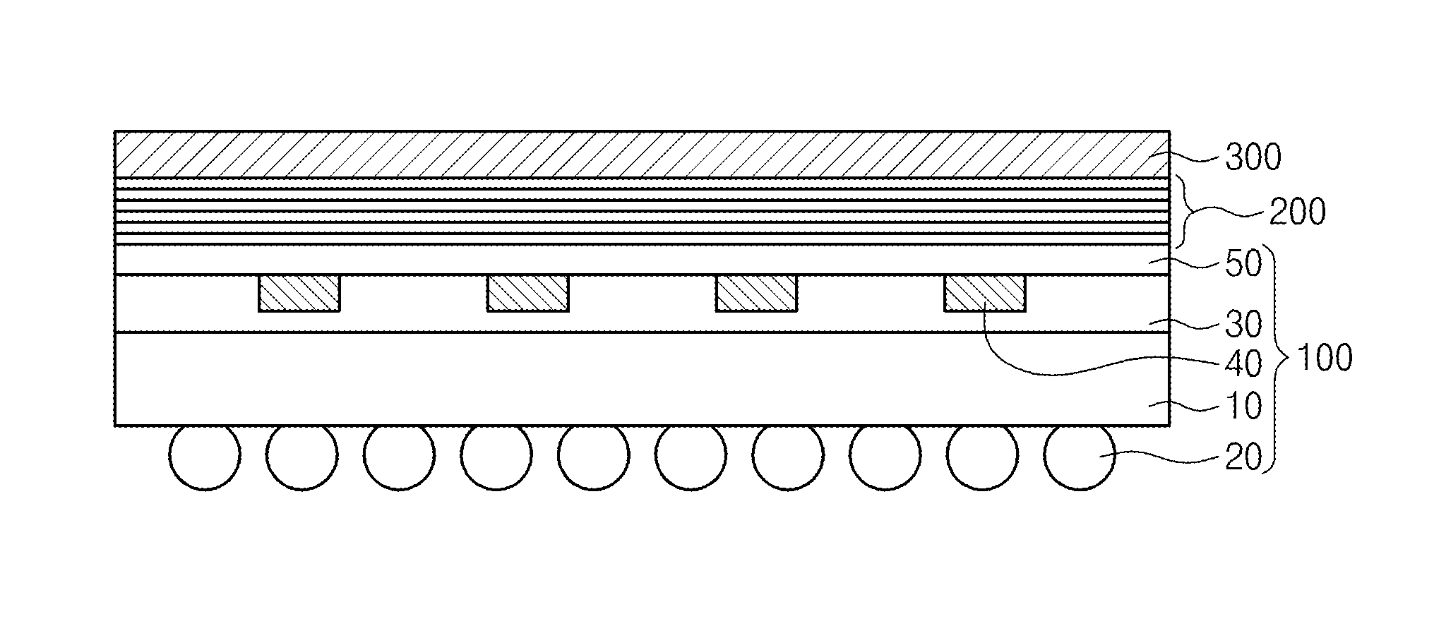
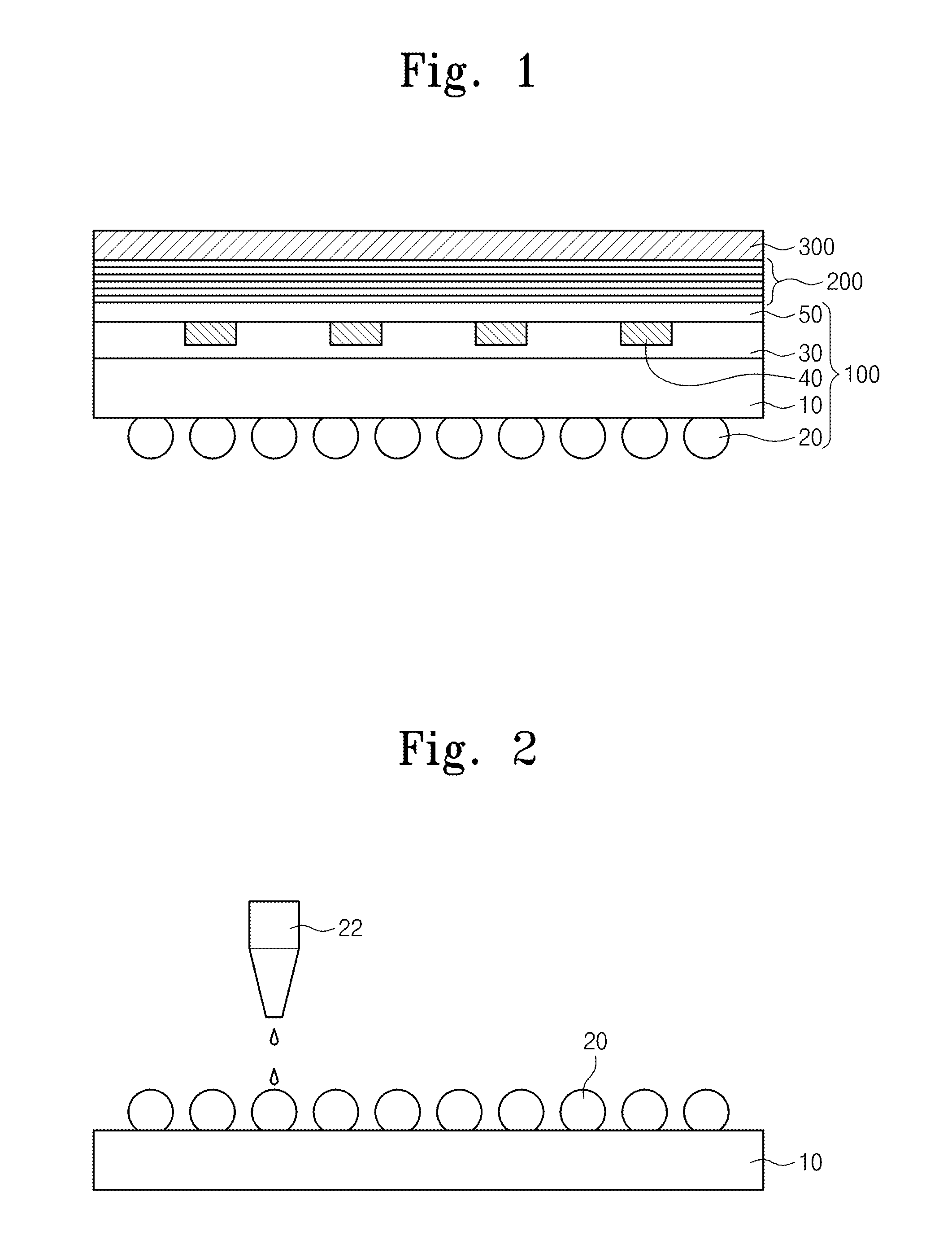
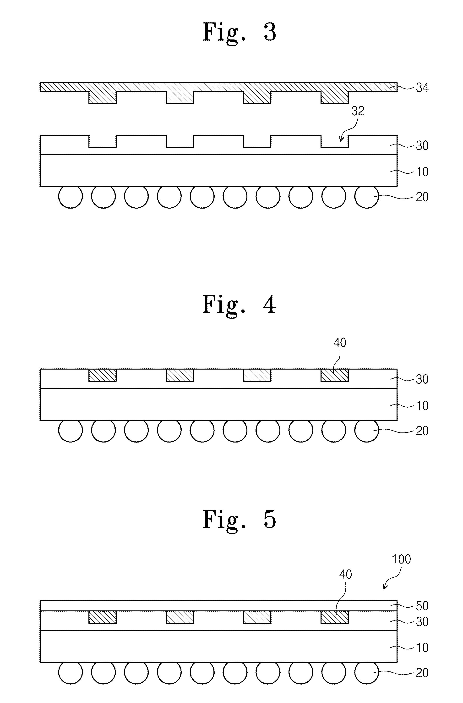
[0037]FIGS. 2 to 5 are cross-sectional views illustrating a method for manufacturing a flexible electrode substrate according to the inventive concept.

[0038]Referring to FIG. 2, the microlens array 20 is formed on a lower surface of the substrate film 10. The substrate film 10 may include plastic or polymer having excellent transparency. The microlens array 20 may be printed to be embossed on the lower surface of the substrate film 10 by using an inkjet technique. The microlens array 20 may include a polymer or plastic having a refractive index which is the same as or higher than that of the substrate film 10. The polymer or plastic may be printed on corresponding locations on the substrate film 100 through a nozzle 22. The polymer or plastic may be regularly embossed, due to self aggregation thereof, on a surface of the substrate film 10.

[0039]Referring to FIG. 3, the transparent mold layer 30 having a trench 32 is formed on the substrate film 10. The transparent mold layer 30 may ...

second embodiment

[0048]Therefore, according to the manufacturing method of the flexible electrode substrate according to the inventive concept, the productivity may be increased or maximized.

[0049]FIGS. 11 to 14 are cross-sectional views illustrating a method for manufacturing a flexible electrode substrate according to a third embodiment of the inventive concept. FIG. 15 is a cross-sectional view illustrating an organic light emitting diode formed by using the manufacturing method of the flexible electrode substrate according to the third embodiment of the inventive concept.

third embodiment

[0050]Referring to FIG. 11, the microlens array 20 is formed to be engraved on the lower surface of the substrate film 10. The substrate film 10 may include plastic or polymer having high transparency. The microlens array 20 may be printed on the lower surface of the substrate film 10 by using the stamping technique or roll-to-roll technique. The microlens array 20 may include a polymer or plastic having a refractive index which is the same as or higher than that of the substrate film 10. The microlens array 20 may include concave parts 24 printed and engraved by a second stamp 26. Therefore, according to the manufacturing method of the flexible electrode substrate according to the inventive concept, the productivity may be increased or maximized.

[0051]Referring to FIG. 12, the transparent mold layer 30 having the trench 32 is formed on an upper surface of the substrate film 10. The transparent mold layer 30 may include a transparent polymer such as polymethyl methacrylate (PMMA), p...


PUM


Abstract

Provided is a method for manufacturing a flexible electrode substrate. The method includes forming a microlens array under a film, forming a transparent electrode layer on the film so as to oppose the microlens array, and forming a grid electrode between the film and the transparent electrode layer or on the transparent electrode layer. Herein, the grid electrode and the microlens array are formed on the both sides of the film by performing at least one of an inkjet printing process, a roll-to-roll printing process, a screen printing process, and a stamping printing process.

Description

CROSS-REFERENCE TO RELATED APPLICATIONS[0001]This U.S. non-provisional patent application claims priority under 35 U.S.C. §119 of Korean Patent Application No. 10-2011-0113006, filed on Nov. 1, 2011, the entire contents of which are hereby incorporated by reference.BACKGROUND OF THE INVENTION[0002]The present invention disclosed herein relates to a flexible electrode substrate, and more particularly, to a flexible electrode substrate of a light-emitting diode.[0003]Recently, it has received great attention to develop a technology for manufacturing a flexible and stretchable electronic device by mounting an electronic element on a plastic substrate. For instance, a flexible display, a flexible solar cell, a flexible RFID, and the like are manufactured by mounting electronic elements on a plastic substrate. Although there are various types of the flexible display, it is considered to be one of the most difficult and high potential techniques to manufacture a flexible organic light emi...

Claims


Application Information

Patent Timeline
Patent Type & Authority Patents(United States)
IPC IPC(8): H01L51/52H01L51/00
CPCH01L51/5275H01L51/0097H01L51/5206Y02E10/549Y02P70/50H10K77/111H10K50/814H10K50/858H10K71/00H10K50/81
Inventor KOO, JAE BONYOU, IN-KYUYANG, YONG SUKKIM, MINSEOK
Owner ELECTRONICS & TELECOMM RES INST
Learn More